After silicon: What will power computing for the next 10 years and beyond?

From 3D chips and carbon-based transistors, to photonics and memristors...
The computer industry is not known for standing still. Moore's Law, coined by Intel co-founder Gordon Moore, famously states the number of transistors that can be inexpensively packed onto a chip doubles roughly every two years - a principle that has held true since at least 1975.
Silicon transistors underpin the whole of modern electronics. With millions on a modern integrated circuit, they are the tiny binary switches working in unison that enable our machines to perform complex calculations at such high speeds.
Invented in 1947 by Bell Laboratories, early transistors were discrete electrical components that measured more than a centimetre across. In the decades since their invention, transistors have been getting smaller and smaller, moving from separate components placed on circuit boards to being fabricated directly on silicon wafers as part of the integrated circuit upon which our digital infrastructure is built.
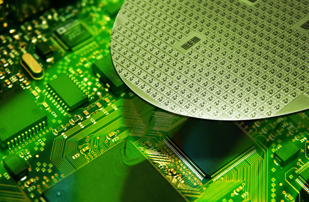
As many as two billion transistors can be packed onto each silicon wafer
(Photo credit: Shutterstock)
Today, Intel sells a microprocessor with two billion transistors crammed onto it - with each one measuring just 65 nanometres (nm) wide. A nanometre is one billionth of a metre. Even smaller transistors - 32nm and 45nm wide - have also been commercialised. Intel's not stopping there either. It has 22nm transistors in its pipeline, and is sizing up even smaller gates in the years ahead.
However, increased transistor density is dogged with questions about how to manage heat extraction. With more and more energy required to power the chips, the amount of heat generated also rises, requiring chipmakers to come up with novel ways to extract it or risk chip and device malfunction.
Shrinking the size of transistors to pack more onto a chip has been the mechanism driving the computer industry for decades, enabling smaller, faster and more powerful hardware to appear every few years. But Moore's Law as it stands can't go on indefinitely. Miniaturisation can only go so far before it reaches the ultimate, atomic limits.
Molecular-scale production could become possible in the next decade, allowing individual atoms to be precision-placed to build transistors measuring just a few nanometres across. Even so there comes a point when scaling silicon effectively bottoms out, owing to problems such as electron tunnelling - a quantum mechanical phenomenon that means transistors with gates less than 5nm wide become unreliable.
With the current silicon-based transistors heading for the atomic end of the line, new techniques and technologies will be needed to underpin tomorrow's computing hardware.
Creating 3D chips
One idea being examined to extend Moore's Law is to layer microprocessor cores on top of each other, increasing the density of transistors by building 3D chips rather than scaling down individual transistors.
Such 3D chips would be made by stacking layers of silicon circuits on top of each other, joined using vertical copper interconnects, known as through-silicon vias (TSVs).
However, stacking silicon is no layer-cake walk. There are many design challenges facing TSVs, which include heat extraction; reducing chip bulkiness and mechanical stress; and the need for industry to agree on standards so chips can be designed and built in existing fabs.
Stan Williams, founding director of the Information and Quantum Systems Lab at HP Labs, is rather downbeat about the prospects for 3D silicon chips, describing them as ...
... long sought after but still out of reach. "That's been a holy grail of silicon for decades and it still doesn't work very well because silicon needs single crystal," he said.
Alternative materials
Another approach for extending Moore's Law is building transistors from alternative materials - in other words, moving beyond silicon. Graphene is among the carbon-based alternatives attracting attention, and scientists have been tinkering with it for several years.
Graphene-based transistors hold the promise of speeding up transistors because of the material's conducting properties, which make it superior to silicon. With graphene, electrons are able to travel faster and thus transistors switch more quickly.
Graphene also has a size advantage. In 2008, a team of scientists at Manchester University demonstrated it is possible to create sub-10nm transistors from grapheme, which unlike silicon remains highly stable and conductive even when carved to just 1nm wide. Consequently, the material could be used to fashion incredibly tiny transistors, perhaps the smallest functioning ones possible.
Earlier this year IBM made a prototype graphene-based transistor. The company demoed it operating faster than silicon transistors of a similar size - claiming the carbon-based component has the potential to operate at 100GHz, compared with up to 40GHz for similarly-sized silicon transistors.
IBM believes the methods used to produce the prototype transistor would be compatible with existing semiconductor fabrication processes - a factor that's likely to be a big influencer in the choice of any silicon replacement.
But despite all this excitement, graphene transistors realistically replacing silicon in integrated circuits remain years away as the chipmaking industry has to create the tools to work effectively with the new material and with nanometre precision.
Other challenges facing graphene transistors include producing high-quality graphene sheets reliably and cost-effectively, along with the ultimate need for production to be integrated into existing silicon-based fab processes.
Carbon nanotubes
Meanwhile tiny tubules of carbon known as carbon nanotubes (CNTs) - about 4nm wide - are another new material that has been probed with interest for several years.
CNTs are super-conductive at room temperature, meaning they could operate at very high speeds with low power - thereby giving them bags of potential as a transistor material.
Both IBM and Intel have been playing around with CNTs for a while. Again, however, a lot of groundwork remains to be done before CNTs could become a viable alternative to silicon transistors in integrated circuits.
Among the challenges for CNTs are questions about how to precision manipulate thousands of CNTs to arrange them in configuration on the chips.
But perhaps the biggest challenge to any silicon alternative is...
...just that: it's not silicon. While there has been lots of industry interest in graphene and CNTs, chipmakers' love affair with silicon is not about to disintegrate overnight. There is simply too much invested in silicon-based fabrication for that.
The photon option
Another big swathe of research is focusing on replacing electrons with photons - that is, using lasers to transmit and process data, rather than electricity.
"Nearly all... movement of data - occurs over copper wires and uses electrical pulses," said HP's Williams. "The issue about that is that the electronics require a huge amount of energy to move that data. They generate a tremendous amount of heat, and that information transfer right now is a major bottleneck for computing and so we're working on what we call photonic interconnect, which is moving data around - actually at any length scale longer than a few millimetres - using light pulses."
Optical computing could help remove bottlenecks in computer hardware by enabling faster data transmission and processing, reduced waste heating and perhaps even leading to smaller hardware. The energy consumption of devices may also be improved in some scenarios.
Optical computing components have already been manufactured, using materials such as germanium, but chipmakers have of course been holding out for integration with their favourite semiconductor - which looks to be on the way.
Intel recently announced a 50Gbps prototype silicon photonics data link with integrated lasers, which looks promising for a marriage of optics and silicon. The company says the 50Gbps data rate is just the starting point for the technology, anticipating its system supporting up to 1Tbps in future.
Intel's silicon photonics data-link prototype with integrated lasers
(Photo credit: Intel)
"What could happen if we take the benefits of silicon manufacturing - the ability to do high volume, low cost - to do highly integrated silicon processing and combine that with the laser that gives us the benefits of very high bandwidth, the benefits of very long distance communication, the immunity to noise, what could happen if we combine those two?" said Mario Paniccia, an Intel fellow and director of the company's Photonics Technology Lab.
Intel's vision is that fibre and photonics will ultimately be able to replace copper for data transmission between chips and between devices - enabling high-bandwidth transmission at low cost and even enabling new configurations of internal computer components such as memory and CPU in the process.
Copper supports data rates of about 10Gbps before a trade-off is required to drive it higher: either by reducing the length of the copper cables, or using more energy to push the electrical signal through, both factors that put shackles on current computing hardware.
By making greater use of photonics, however, Paniccia believes...
...hardware could be designed differently. Components would no longer need to be crammed together, enabling a cooler working environment and reducing component and device failure rates.
Intel: "In the future everything will be connected by fibre..."
(Photo credit: Shutterstock)
"We believe that as we move into this next era of driving optical communications as a technology into the platform we're going to revolutionise the way we design PCs and servers, the way we design future datacentres and the way data is moved in and out of future cloud computing," he added.
HP's Williams also believes photonics will also be doing great things to the guts of our electronics - speeding data around while also cutting waste heat and electricity bills.
"You're able to get much higher bandwidth - in other words the frequency with which you can transfer information is much higher, you get much shorter latency - you don't have to wait as long for the signal to arrive, and you get both of those at much lower power, so you're not generating a lot of heat and of course it doesn't cost you as much to run the datacentre in the first place," he notes.
So how long will we have to wait for a fibre-based electronics boost? Not as long as you might think. "This is not a technology that we think is 10 years out," Intel's Paniccia said. "I think you will see silicon photonics type commercialisation in the next three to five years."
"We're aggressively driving this to commercialisation so I think by the middle part of this next decade you will see integrated silicon photonics in and around our platform," he added.
It's a confidence that HP's Williams shares, noting: "I'm hoping that we're going to have an HP product with photonic interconnect inside it in the next two to three years."
But if the prospect of photonics wasn't exciting enough, there is an even more radical transformation that could be coming in the not-too-distant future if a new type of electrical circuit element lives up to its promise. Meet the memristor.
HP's memristor - the fourth circuit element?
(Photo credit: HP Labs)
The memristor is a device first postulated in 1971 by US electrical engineer and computer scientist Leon Chua that, up until two years ago, remained just so much theory on paper.
However, in 2008, Williams and his team at HP caused much excitement in the electronics world by developing the first solid-state memristor.
Why all the excitement? A memristor is a nanoscale circuit element that can act as both a storage medium and a logic gate, meaning it can be used to perform a computation and store the result - a radical conflation of electronics properties that makes memristors resemble synapses in the brain, according to Williams.
Used in conjunction with transistors and photonic interconnects, he believes memristors could...
...extend the power principle of Moore's Law for decades to come - without having to keep playing the shrinking game.
Memristors could lead to a radical shake-up of circuit board architecture
(Photo credit: Shutterstock)
"The word itself - memristor - is a contraction of memory resistor so this is a device that stores history," he told silicon.com. "It remembers its past. What that means is that it can be used as either a memory device - similar to a DRAM memory - or a storage device, as magnetic hard disks are used today. But the fact is that this is a single device that can be used for either purpose because it is non-volatile. Once it learns something it doesn't forget unless that information is erased."
The memristor has radical implications on the memory and storage front - but add in its ability to crunch data on-demand and Williams reckons it's truly revolutionary.
"This is a single device that can either be used to store a bit of information or to compute a Boolean logic function," he said. "So here all of a sudden you have the possibility of having, for instance, a chip with just a whole bunch of memristors on it and those memristors can either be used as long-term storage, short-term memory or even as a computing element - as a logic gate - and you can define what you want those memristors to be when you want them to be... You can even do a computation and then just store the result of the computation on the device that did the logical operation.
"That's completely different from the way current processors and memory work," he added.
So what does such a device mean at the business end of computing? Zero boot-up time for a start, according to Williams.
"This ability to provide non-volatile memory at densities that vastly exceed anything that can be achieved by DRAM - but also having this random access of DRAM - is going to make a huge difference in terms of the efficiency of future computing machines," he said.
"It means that we're not going to have to wait a long time for information to have to move back and forth between hard disk and memory - and also I think that, for a consumer, it will mean no more boot-up and no more boot-down."
He continued: "You have the ability to collapse the memory and storage hierarchy. You no longer have a spinning hard disk, you no longer have separate storage and memory but it collapses onto a single system. And then eventually it can even collapse on to the same chip where the computation is performed."
And with the prospect of conflating computing function onto fewer components, more efficient hardware that requires less energy to fire it up becomes possible. This development in turn leads to a...
...virtuous circle where batteries last longer, and devices can be smaller - and all because of the memristor's ability not to forget when you switch it off.
"You could have certain types of devices that would never even need to be recharged," Williams said. "A significant fraction of the weight in so many computer systems now is the battery and then you've got to lug around the cable and the transformer for recharging it. So there's a lot of things that could be done to vastly increase the efficiency of the system and get more computing power out or more computing capability out for less electrical power in. That I think is just going to lead to a lot of extra convenience and it's just better for the planet."
Williams envisages HP being able to bring a memristor-based thumb drive to market in about three years to compete with flash memory - and then in about five years he reckons on memristor-based products competing with magnetic hard disks. Shortly after that he believes memristors could compete with DRAM for the main memory in computers.
Memristor-based products could compete with flash drives in three years, says HP
(Photo credit: Shutterstock)
"It's probably the 10-year timeframe that we'd actually be seeing chips where the memristors themselves would be doing at least some of the computing in the systems," he added.
They would not replace transistors entirely, since transistors are still required to inject energy into the chip as memristors are passive. However, Williams sees hybrid systems incorporating the two circuit elements gradually evolving over the next 10 years.
After that, he believes they will be playing an ever bigger role in our computing hardware, perhaps eventually leading to a single hybrid chip that would perform all the computing and storage in one system.
"That would be a tremendous collapse of the hierarchy that we have today where we have a spinning hard disk, separate memory chips and a processor chip. All of that would essentially wind up being on one piece of silicon with transistors essentially providing the input, output and power and then the memristors providing all the computational functions."
By combining the advantages of silicon-based photonics and memristors, Williams believes Moore's Law doesn't have to come to a stop.
"The photonic communication of information and the capacity for memory and storage that memristors allow... has the very real potential for improving computing technology, or computing efficiency shall we say, by three or four orders of magnitude over what we have today," he said.
"In other words this is the equivalent of Moore's Law - this is not putting...
...more transistors on a chip, this is essentially usually the same number of transistors that we've been using, but getting a lot more out of those transistors by taking away bottlenecks in other areas. The functional equivalent of Moore's Law can go on for another 20 years without actually scaling and making smaller transistors by this combination."
And even beyond that, memristors have potential in Williams' view - owing to their ability to compute in a non-digital way, something he says is closer to how a synapse functions in the brain. Tapping into this could expand compute power in areas machines have traditionally struggled with but which brains excel at, such as identifying a familiar face.
HP: Memristors compute in a non-digital way, similar to synapses in the brain
(Photo credit: Shutterstock)
"You have the very intriguing possibility that we start to build computers that are no longer working in the digital domain but are essentially performing at least some forms of computation - such as facial recognition - or performing logical functions or learning how to perform a task, rather than being programmed to handle a task, effectively using memristors as electronic synapses."
"There are certain things brains can do that are many, many, many orders of magnitude more efficient than digital computers can do," added Williams.
As well as excelling at these compute and memory-intensive tasks, memristor-based machines could be used to study theories of brain architecture and emulate brain function.
Another quirk of memristors that adds to their appeal is their ability to stack - making 3D memristor-based circuits "practically trivial" to build, says Williams, unlike current computing's transistor-only circuits.
"In our lab we have built memristors with 3nm feature sizes so we know that it can scale down to that level but the other thing about memristors is it's what's called a thin-film technology. We don't require single crystal silicon for memristors and so we can stack many layers of memristor circuits on top of each other by fab processes," said Williams.
"Not taking chips and stacking chips on top of each other but in the fab we can make multiple layers of memristors on top of each other."
He continued: "In the end if you're talking about number of devices per square centimetre or number of devices on a single chip, memristors can scale to vastly higher numbers than transistors can, because they are trivially stacked and they can be much smaller than a transistor, so you can have a smaller device and you can stack it so that the number of devices on a chip can be factors of a thousand more memristors than transistors on a chip.
"And perhaps if you just want to continue talking about Moore's Law being number of devices on a chip, maybe it just becomes the number of total devices - memristors and transistors - that you count."
Whatever electronic innovations prevail, the principle of ever-improving hardware looks unshakable for the foreseeable future - and the spirit, if not the letter, of Moore's Law means we can look forward to faster, more capable hardware for years to come.
"For 40 years in some sense we've had it very easy - our electronics and our computing machines have gotten exponentially better, exponentially more capable simply because we were able to make transistors smaller," Williams said.
"And so because that was so easy... it was very cost-effective, that's what we did. Well, those days are over frankly, but there's absolutely no cause for alarm or panic because what that's meant is - especially over the past decade - people have anticipated this and a huge number of brilliant ideas have come up for being able to improve other aspects of computing to bring them up to the level of what transistors are.
"The memristor and the photonic interconnect are both transformational technologies - each one by itself would be huge but the two together are really going to be driving computing for a good 20 years."
Electronic innovation will ensure that computing will continue to speed up
(Photo credit: Shutterstock)