ARM unveils low-power chip for the internet of things
The changes made to improve power consumption in the M0+ microcontroller chip are set to be rolled out across ARM's entire range of embedded processors, cutting the electricity cost of the 'internet of things'
ARM will bring the power saving techniques used in its Cortex M0+ microprocessor to its entire range of embedded chips, cutting the power needs of the 'internet of things'.
The changes made to improve power consumption in the M0+ microcontroller chip are set to be rolled out across ARM's entire range of embedded processors.Image credit: ARM
ARM started licensing the Cortex M0+ chip design, which the Cambridge-based company calls 'the world's most energy-efficient microprocessor', to chip manufacturers on Tuesday.
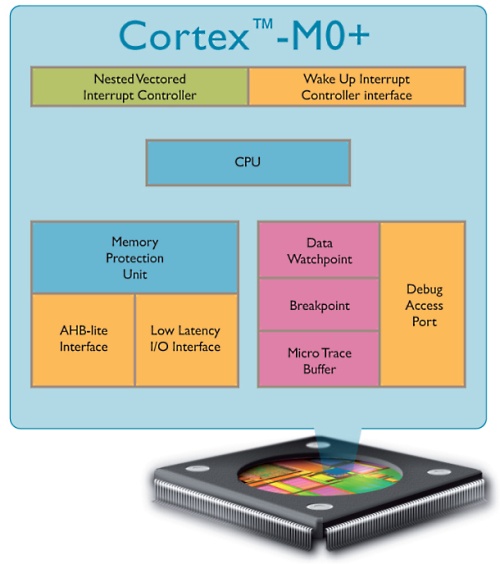
The chip die is 1mm2 and consumes "around one-third of the energy of any 8- or 16-bit processor available today, while delivering significantly higher performance", the company said. An M0+ processor takes nine microamps per MHz when made in a 90nm process, and is intended to run at speeds between 5MHz and 50MHz.
The M-class of processors is designed to let companies add capable microcomputers to utility meters, cars, white goods (washing machines, fridges, microwaves and so on) and industrial devices, to collect data, react and, in particular, communicate — a term sometimes called machine-to-machine (M2M) communication, or the internet of things.
The European Union has separately funded the IERC — the Internet of Things European Research Cluster— via the Seventh Framework Programme to investigate new technologies.
Power consumption
Thomas Ensergueix, a CPU product manager at ARM, said the company hopes that by cutting the power consumption of the chip and giving it a 32-bit capability, more advanced communications protocols can be used by machine-to-machine devices, while drawing less power.
"When it comes to running [M2M] communications it starts to be very difficult for 8-bit and 16-bit because their communications track is designed for 32-bit," he said. "You can implement them on 8- and 16-bit but will really slash down your low power advantages... the nice thing about M0+ is you can manipulate 32-bit addresses and 32-bit data." IPv4, the current default internet protocol, is based on 32-bit addresses.
The nice thing about M0+ is you can manipulate 32-bit addresses and 32-bit data.
– Thomas Ensergueix, ARM
Ensergueix said the company cut the power use of the chip by reducing the steps in the instruction execution pipeline from three to two, thus reducing the number of gates; by using more clock gating to suspend inactive circuts; by improving how the processor interacts with the memory; and by introducing a feature that powers down all internal debugging if no debugger is connected.
"We aim to refresh in the next year the Cortex M portfolio and here we intend to use all the [M0+] improvements which have proven to have brought our customers forward to the M3 and M4 [series]," he said. "Now if you are able to reduce the pipeline for the M3 and M4 to two stages, it could be questionable... people are talking about much bigger instruction sets... as for the flash or better clock gating or the debug, these are things which could indeed be very interesting."
Processing versus energy
By reducing the execution pipeline from the three stages — fetch > decode > execute — to two stages — fetch and pre-decode > post-decode and execute — ARM is sacrificing a little processing performance for better power consumption.
"When it comes to execution, the rate [is] around five to 10 percent below previous [chips with the M architecture]," Ensergueix said. However, this does not have too much of an impact because on a 90nm process the M0+ is always limited by external memory speed, he said. M0+'s predecessor, the M0, was adopted by companies from Freescale Semiconductor to NXP and was used in a variety of M2M products, such as a power monitoring chip for datacentres.
The M0+ processor gate count can scale from 12,000 per chip up to 30,000, though ARM expects most people will use around 20,000 to 25,000 gates, Ensergueix said.
The 12,000-gate variant will mostly be used as a companion processor; 'not being the main brain,' he said.
Though ARM has listed the dynamic power use for M0+ chips made to a 180nm, 90nm and 40nm process on its website, Ensergueix admitted power leakage below 90nm is so severe that "static consumption is reaching the level of the dynamic consumption".
"In terms of static consumption the smaller the processor, the higher consumption you'll have for leakage. It's become very challenging beyond 90nm to keep very good static consumption," Ensergueix said.
Get the latest technology news and analysis, blogs and reviews delivered directly to your inbox with ZDNet UK's newsletters.