IEDM 2017: GlobalFoundries announces 7nm chipmaking process

In a late addition to this year's IEDM 2017 lineup, GlobalFoundries unveiled details of its 7nm process which promises a significant increase in density, performance and efficiency in comparison to the 14nm technology used to manufacture AMD processors, IBM Power server chips and other products. GlobalFoundries will start 7nm production using current lithography tools, though it plans to quickly move to next-generation EUV lithography to cut costs.
Based on GlobalFoundries latest generation of 3D or FinFET transistors, the 7LP process has a fin pitch (the distance between the conducting channels) of 30nm, gate pitch of 56nm and a minimum metal pitch of 40nm--all of which are "significantly scaled from 14nm." GlobalFoundries said it tuned the fin shape and profile for best performance, but did not provide measurements for the width or height of the fins. The smallest high-density SRAM cell measures 0.0269 square microns.
These feature sizes are similar not only to TSMC's 7nm process, but also to Intel's 10nm process, which is roughly equivalent to what the foundries refer to as 7nm. (Samsung will provide details of its 7nm process, which uses EUV from the outset, at ISSCC in early 2018.)
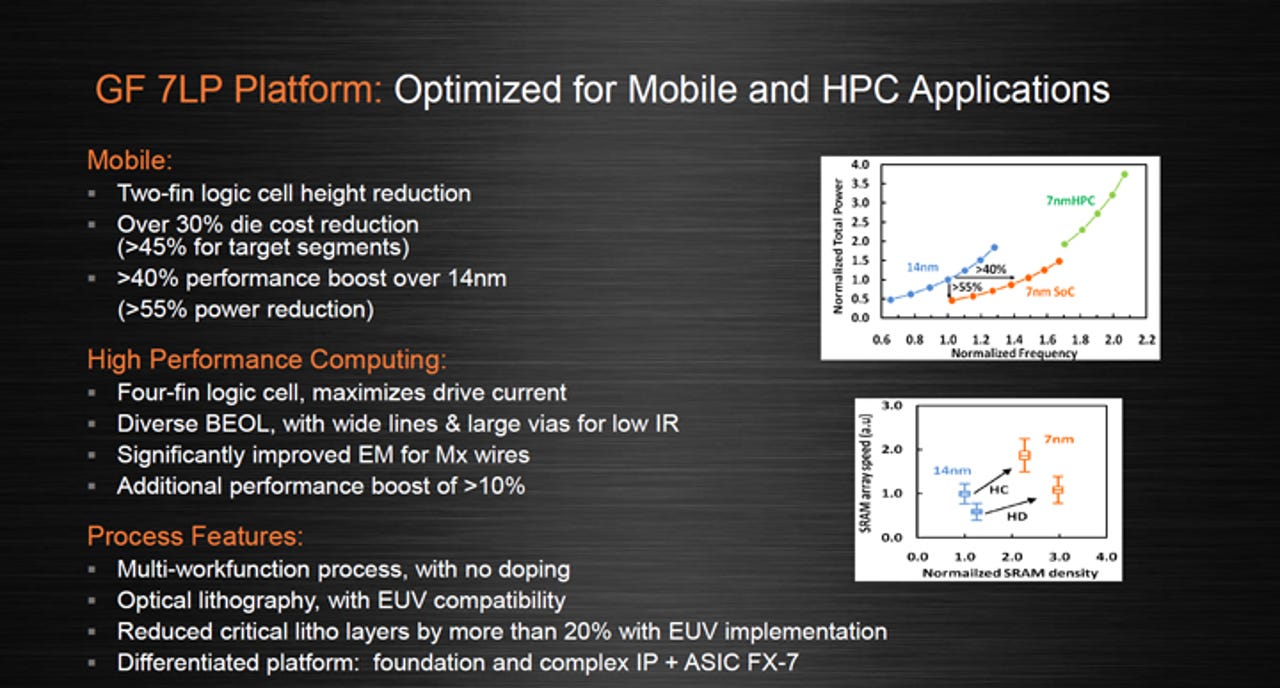
GlobalFoundries will offer two different flavors of 7LP. The high-density standard cell for mobile processors has two fins and is only 240nm tall translating to a 0.36x area reduction at the SoC level compared to 14nm. A separate version for high-performance servers such as IBM Power has four fins, as well as larger contacts and wires, and operates at a higher frequency.
Overall GlobalFoundries is promising a 2.8x increase in density, and either a 40 percent boost in performance or 55 percent reduction in power at the same performance. The high-performance version can deliver another 10 percent boost. Those are some impressive numbers, but it is worth underscoring here that GlobalFoundries is comparing this to its current 14nm process (licensed from Samsung) because it is skipping 10nm (though it will offer an interim 12LP process with 15 percent higher density and 10 percent better performance starting early next year). TSMC adopted a similar strategy when it unveiled a 7nm 256Mb SRAM test chip at last year's conference, comparing it to its current 16nm process rather than what it says will be a "short-lived" 10nm node.
Like Intel, GlobalFoundries will use self-aligned quad patterning (SAQP) to fabricate the fins, as well as double-patterning for metal layers, and has introduced cobalt metal contacts to reduce resistance. As a pure-play foundry, it will offer a wide range of metal stacks for different applications. The technology also supports a range of threshold voltages (the gate voltage at which the device turns on) without doping, which GlobalFoundries says improves performance and reduces variability.
GlobalFoundries plans to introduce EUV lithography in two stages. First, it will use EUV only for contacts and vias, cutting more than 10 lithography steps out of the process to reduce cost without requiring customers to redesign their chips. It will eventually use EUV for several critical layers, a step that will require a redesign but should deliver additional power, performance and area benefits.
The 7LP process will be in trial production in mid-2018, which means it will be volume production in the fab in Malta, New York sometime in 2019. GlobalFoundries said it has multiple product tape-outs--the last major step in the design process before production--scheduled over the next year. The 7LP process is also the basis for its FX-7 ASIC offering, which many customers are using to design specialized high-performance chips packaged with high-bandwidth memory for machine learning workloads.
Of course, not all customers need chips with this level of performance and many applications require lower power. GlobalFoundries has developed an alternative, based on FD-SOI or fully depleted-silicon on insulator, for these applications. FD-SOI uses a different type of wafer substrate that costs slightly more, but the design is simpler and the process involves fewer steps, so the overall cost should be competitive. More important, it can offer performance similar to leading-edge FinFETs while using less power, making it well-suited for applications such as the Internet of Things and application processors for low-end and mid-range phones. "In my personal view, it is ridiculous to think that one process can serve all applications." GlobalFoundries CTO Gary Patton said in an interview.
It has taken some time for the design ecosystem to fall into place, but there are signs that FD-SOI is starting to gain momentum. Samsung already offers a 28nm FD-SOI process (28FDS) with plans for 18FDS, and recently stated it had taped-out more than 40 products. GlobalFoundries, which has 22FDX and plans to follow-up with 12FDX, expects to have 25 tape-outs by the end of 2018. "Competitors like to say that FD-SOI is not gaining traction, but this is not accurate," Patton said.
Patton also talked about GlobalFoundries evolution into a full-service foundry. The acquisition of IBM Microelectronics brought lots of intellectual property and expertise in 3D FinFETs, enabling GlobalFoundries to develop its own 7nm process, as well a leading RF (radio frequency) business for wireless. The Malta fab is in high-volume production at 14nm, and GlobalFoundries operates four additional fabs with a sixth one in Chengdu, China slated to start production next year. While AMD and IBM remain key customers, GlobalFoundries now has design wins across a wide variety of applications such as AI, automotive, 5G wireless and Internet of Things. "In the past, the company had a lot of challenges, but now we have a strong product portfolio," he said.
GlobalFoundries also has a 700-person development team that works with the IBM Research Alliance and Albany NanoTech on what comes after 7nm. At IEDM, the alliance (GlobalFoundries, IBM Research and Samsung Electronics) described its development of functional gate-all-around stacked nanosheets, which it said looks like a promising option at 5nm and beyond.