Inside Apple's A6 processor
Thanks to fuming sulfuric acid, an ion blaster, and a good microscope, we can finally see what makes the iPhone 5 tick.
Apple unveiled a lot of new shiny things during its iPhone 5 event last week, but the Cupertino giant doesn't talk much about what makes its hardware tick. One mystery inside the iPhone 5 was the new A6 processor. Now that an iPhone 5 has fallen into the hands of repair specialists iFixit -- working in association with Chipworks -- we can get a closer look at the new silicon powering Apple's flagship consumer electronics device.
Getting to the heart of the A6 isn't easy. The processor first needed to be decapsulated in a fuming sulfuric acid solution, then a microscope used to examine and photograph the die. Then, in order to dig deeper, an ion blaster, affectionately known as Ibe (short for "ion beam etching") is used to peel away the layers. This allowed some fantastic photos to be taken of the processor.
Read this:
iPhone 5 16GB costs an estimated $207 to build
A 16GB iPhone 5 that Apple sells for $649 only costs the company an estimated $207 to manufacture. Apple also charges an incredible $100 premium for only $10 worth of NAND storage.
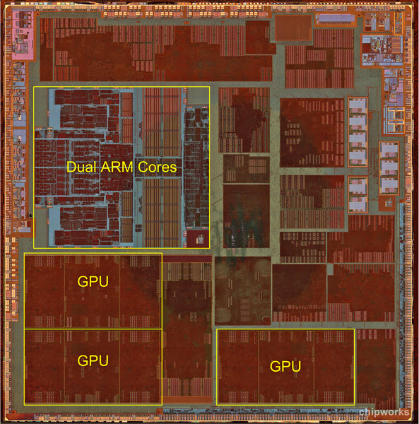
Buried inside the A6 is some interesting technology. First, there are dual ARM core blocks and three PowerVR graphics cores. The teardown of the chip also revealed that the 1GB of RAM on the silicon was supplied by Elpida rather than Samsung, another indication of the growing rift between Apple and Samsung.
Despite the RAM being provided by Elpida, Samsung continues to manufacture the processors for Apple, using its 32-nanometer CMOS process.
The A6 is much larger than the A5 powering the iPhone 4S, swelling to 96.71 mm2. Compare this to the previous-generation A5 which powered the third-gen Apple TV, second-gen iPad 2 and fifth-gen iPod touch, which was only 69.9 mm2. iFixit claim that Apple has manually laid out the ARM core block -- manually as by hand as opposed to using a computer -- in order to maximize performance. But this manual layout comes at a price, being more expensive and more time consuming than allowing computer software to do it.
According to Miroslav Djuric, iFixit's chief information architect, the ARM cores inside the A6 "might be the only manual layout in a chip to hit the market in several years".
iFixit and Chipworks also took their ion blaster to other chips, including the Murata Wi-Fi SoC module, which actually turned out to comprise of a Broadcom BCM4334 single-chip dual-band combo package, fabricated in Taiwan at TSMC on a 40 nm CMOS process. This brings Wi-Fi 802.11 a/b/g/n, Bluetooth 4.0 and HS, and an FM receiver (not used in the iPhone) into a single package.
Another chip to get the fuming sulfuric acid solution and ion blaster treatment was the Qualcomm MDM9615 LTE modem. This allows for multi-spectrums, multi-mode LTE support, which means you can talk on the phone and use data simultaneously.
According to Chipworks, while many of the packages inside Apple's newest smartphone look like old chips on the surface, the "iPhone 5 is not an evolution of design, but quite possibly an entirely new design".
Image source: iFixit/Chipworks.