Inside Intel's Core architecture

It is hard to overstate the importance of the Core micro-architecture to Intel, and thus to the rest of the industry. The product of a major debate within Intel (what Pat Gelsinger, General Manager of the Digital Enterprise Group, called the 'speed freaks versus brainiacs'), it marks the victory of those who felt that extra performance was best achieved not by constantly upping the processor's clock speed, but by going for ever more parallel systems with much finer control of performance versus power consumption.
With the Core 2 Duo and Core 2 Extreme, the Core architecture is being applied to mobile (Merom) and desktop (Conroe) processors, which now join last month's Xeon 5100 (Woodcrest) to put basically the same chip in everything from notebooks to servers.
All modern processors work by reading a stream of instructions that tell them where data is in memory and what to do with it. Originally, processors took in one instruction from memory and took as long as it needed to fully execute it before starting on the next. Each clock tick -- of which there are a million a second with a 1MHz processor, a billion with 1GHz -- moved the instruction one stage further through the processor. Some instructions could take four or more ticks.Now, processors move blocks of hundreds or thousands of instructions into cache before executing them in blocks of four or more at a time, trying to execute even the most complex instruction in one tick. To this end, each generation of processor uses all the best tricks from previous designs and adds some of its own: the Core architecture is mostly a mix of Pentium M (Banias and Dothan) ideas with those from the Pentium Pro/P6. It's a major departure from Pentium4's NetBurst design.
Core details
Core is a pipelined architecture, where instructions move through a number of internal stages between entering the processor and being completed – 'retired', in the jargon. As an instruction exits a stage another can enter, minimising the idle time for each internal component. Core has around fourteen stages in its pipeline: as with most modern architectures, there are a number of complications, such as early completion and out of order execution, which make it hard to define exactly how many stages there are.
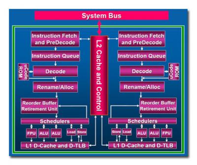
The front end of the machine fetches instructions and does preliminary analysis and reconstruction work on them. Core is a four-wide machine, with portions of five or six wide, meaning it can execute at least four instructions at once. That's wider than any previous x86 architecture. Internally, Core has its own microcode, and the first stage in dealing with x86 instructions is translating them to micro-ops in that microcode while working out which instructions can be safely combined into single operations -- 'macrofusion'.
As with all chip designers, Intel spends a lot of time analysing software, looking for common combinations of instructions -- for example, a mathematical comparison followed by a switch to a different section of code depending on the result of that comparison. By fusing those two x86 operations into a single micro-op, the chip can complete them much faster. This happens on average once every ten x86 instructions.
Core also does 'microfusion', where it does something similar but for those occasions when a single x86 instruction translates into multiple micro-ops. Where possible, the processor binds two of those micro-ops together and treats them as one; again, this can reduce the number of processing steps by around ten percent in some cases.
Once we've got streams of micro-ops rattling through the pipelines, considerable performance gains can be achieved by spotting those instructions that'll take some time to complete and starting them as early as possible. Typically, these involve reads or writes to memory: if you know that ten steps down the pipeline you'll need to load some information in, it's best to send the request out to the relatively slow memory system as early in the pipeline as possible. Unfortunately, instructions already in the pipeline may change the data at the memory location that you've preloaded, making your version out of date by the time it comes into play.
Core copes with this by using prediction hardware that allows a read from memory to happen even if there's a write already in progress, provided the predictor thinks that the write is unlikely to cause a problem. Checking afterwards catches the times that this prediction is wrong, when there's a relatively slow process of recovering the right information; however, on balance the gains from guessing right outweigh the losses when it gets it wrong.
By the time instructions reach the end of the pipeline, they will have been operated on in any order that the chip deems most efficient. It has a single unified scheduler that decides what happens when, and that controls every execution unit on the chip.
Finally, the retirement unit or reorder buffer takes the results of all of the efficiently scrambled, reordered and smashed-up instructions, and rebuilds the results as if they'd in fact been operated on by an old-fashioned processor that took in one instruction, carefully obeyed it step by step, and produced the results before starting on the next one. The retirement unit is one of the most complex parts of the chip; even the architects themselves are prone to calling it 'magic'. That's not so far from the truth, as it is responsible for maintaining the illusion that everything happens in strict order while disguising the massive manipulation that's going on elsewhere.
Shared cache, dynamic power management
All of the above is true separately for each core, each of which operates entirely independently of the other. They share their Level 2 cache, though, and this is where Intel has optimised operations for the simultaneous use of both cores. This means that when both cores are operating on the same area of memory, just one copy of the data is needed in the cache, increasing efficiency and leaving more cache for other processes. The cache also dynamically allocates how much is used by each core, so that if one is idle or operating in a slow, low-power mode, more cache is available to the other.
Underlying all this is Intel's dynamic power management. Areas of the chip that aren't needed at any particular point can be disconnected from main power, while others are switched into low-power modes when they don't need to deliver full performance. This extends to buses, which can be split so that parts not needed are powered down without affecting the rest, and the cache, which puts parts of itself into low-power modes that maintain their contents but react only sluggishly when this wouldn't affect performance.
From notebooks to servers
The overall effect of this level of control, combined with Intel's transistor architecture, which can work alongside a wide range of performance versus power-saving schemes, means that the same architecture can be used from notebooks to servers by setting some easily configured variables such as bus speed, cache size and supply voltage variations. With its impressive benchmarks and Intel's promise to aggressively introduce new products based on it, Core deserves to be at the heart of the company's strategy.
| Core 2 Duo Desktop processors | ||||
| Processor | Clock speed | Bus speed | Level 2 cache | Price |
| Core 2 Duo Extreme X6800 | 2.93GHz | 1066MHz | 4MB | $999 |
| Core 2 Duo E6700 | 2.66GHz | 1066MHz | 4MB | $530 |
| Core 2 Duo E6600 | 2.40GHz | 1066MHz | 4MB | $316 |
| Core 2 Duo E6400 | 2.13GHz | 1066MHz | 2MB | $224 |
| Core 2 Duo E6300 | 1.86GHz | 1066MHz | 2MB | $183 |
| Core 2 Duo Mobile processors | ||||
| Processor | Clock speed | Bus speed | Level 2 cache | Voltage |
| Core 2 Duo T7600 | 2.33GHz | 667MHz | 4MB | 1.0375-1.3V |
| Core 2 Duo T7400 | 2.16GHz | 667MHz | 4MB | 1.0375-1.3V |
| Core 2 Duo T7200 | 2.00GHz | 667MHz | 4MB | 1.0375-1.3V |
| Core 2 Duo T5600 | 1.83GHz | 667MHz | 2MB | 1.0375-1.3V |
| Core 2 Duo T5500 | 1.66GHz | 667MHz | 2MB | 1.0375-1.3V |