The race to the FinFETs

The demand for smartphones and tablets with better performance and longer battery life has been driving the industry to come up with chips that are faster, smaller and use less power. To remain on this treadmill known as Moore’s Law, chipmakers have in recent years relied on a series of technological breakthroughs, most recently 3-D transistors known as FinFETs.
Intel started production with FinFETs in late 2011 with its 22nm Ivy Bridge processors and since then it has shipped more than 500 million chips. These are mostly for PCs and servers, though it is on target to ship 40 million tablet processors this year, and it is offering the technology to other customers as a foundry. Now the other foundries, which manufacture chips for customers such as Apple, Qualcomm, Samsung and MediaTek, are scrambling to catch up.
In the past week TSMC, the world’s largest contract chipmaker, has made two announcements meant to signal its progress on FinFETs. First, TSMC said it had produced a working network processor, with 32 ARM Cortex-A57 CPU cores, for HiSilicon, the chip division of Huawei. Then, earlier this week, the foundry announced that a 64-bit ARM big.LITTLE test chip manufactured on its 16nm FinFET process delivers sustained speeds of 2.3GHz with its big Cortex-A57 cores and uses only 75 milliwatts of power with its little A53 cores on typical applications.
The first batch of chips will be manufactured using what TSMC calls 16FF. This process was qualified in November 2013 and the first products were taped-out in April. (Tape-out is the last major step in the design process before actual production.)
Featured
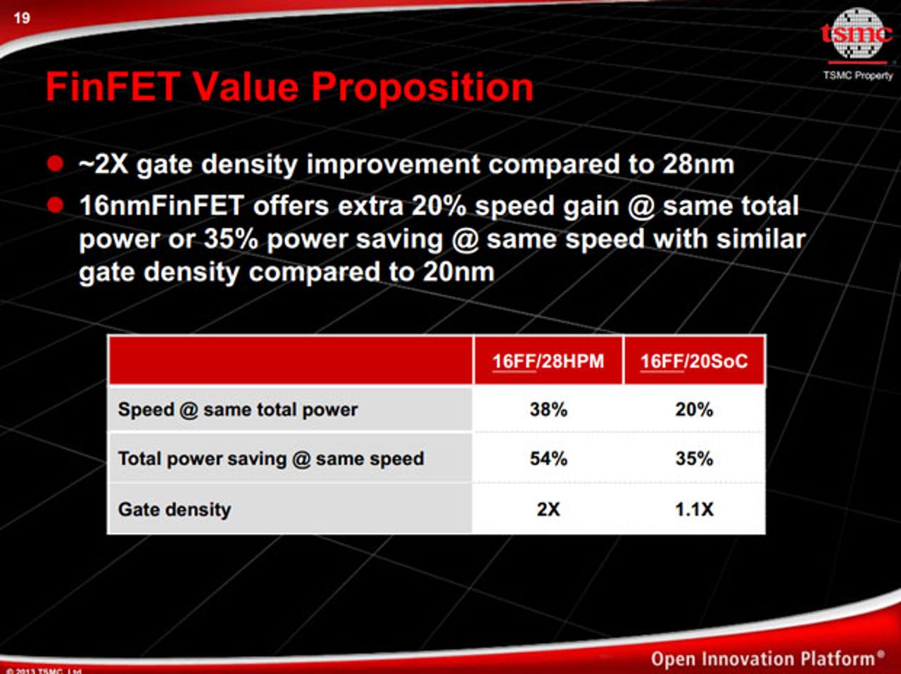
The foundry plans to quickly follow up with an enhanced version, known as 16nm FinFET plus or 16FF+, which will provide another 15 percent boost in performance or 30 percent lower power than 16FF. The 16FF+ process will deliver a 40 percent increase in transistor performance compared to its 20nm process with conventional planar transistors, and it will match the performance of 14nm FinFET transistors from competing foundries, according to TSMC. The 16FF+ process should be ready for customers by the end of the year, which means the first tape-outs will likely be in early 2015.
The foundry is currently in what it calls risk production, working on 15 products this year and another 45 chip designs next year including mobile application processors, cellular basebands, consumer SoCs, GPUs, network processors, programmable logic, and CPUs for PCs and servers. The bulk of these will be based on the second-generation 16FF+ process.
TSMC has been doing well with its current 28nm process — in large part because it chose a different approach to planar HKMG (high-k metal gates) that delivered better results — and it is in the process of what it says is the fastest ramp in its history to 20nm (20 percent of revenues this quarter).
TSMC chose 16nm, which uses smaller transistors but has the same back-end metal layers, as a sort of stepping stone to ease the transition to FinFETs. It won’t provide the area scaling benefits of a typical shrink, but it does boost performance and power. It also uses 95 percent of the same tools as 20nm planar, and on a quarterly call in April, the foundry said yield was improving so quickly that it had already caught up with 20nm.
So it is surprising that 16nm FinFETs won’t be in volume production until late 2015. On the quarterly call in July, Chairman Morris Chang conceded that TSMC would lose a little leading-edge share to competitors with 14nm FinFETs next year, and said the foundry was already shifting its focus to 10nm. TSMC has said that 10nm will deliver another 25 percent speed boost at the same power or a 45 percent reduction in power at the same speed over 16FF+. Just as important, it will be a true shrink delivering 2.2x the transistor density. To underscore this, TSMC and ARM announced today that they will be working together on the next node and hope to have the 10nm FinFET process ready for tape-outs by the end of next year.
Samsung seems to be moving more quickly on FinFETs. With an assist from Cadence, Samsung taped out its first 14nm test chip, a Cortex-A7 processor, in December 2013. The process, known as 14LPE, was qualified in February; and the foundry has completed tape-outs of multiple products and has already started early commercial production for some customers, according to Kelvin Low, the marketing manager for Samsung’s foundry business.
In comparison to 20nm planar transistors, the 14LPE transistors will deliver either a 20 percent boost in performance or a 35 percent reduction in power. At the Design Automation Conference in June Samsung first demonstrated a reference board with a working 14nm ARM processor and it has been showing the demo at ARM TechCon this week. A higher-performance version, known as 14LPP, will be qualified in a couple of months and Low said multiple customers are close to taping out the chip's first designs.
Back in April GlobalFoundries announced it would give up on developing its own 14XM process and license Samsung’s 14LPE and 14LPP processes. GlobalFoundries said Samsung’s version was further along in development and provided higher density. The two companies said that 14nm chips will be up to 15 percent smaller than those manufactured on a 20nm planar process, while TSMC’s 16nm FinFET process will deliver no scaling benefit over 20nm.
The move also provides a second source for 14nm chip manufacturing, which can be attractive to customers. The 14nm chips will be manufactured at two Samsung fabs, S2 in Austin, Texas and S3 in South Korea, and at GlobalFoundries’ Fab 8 in Saratoga, New York. GlobalFoundries is already producing test chips, and it expects to have customer tape-outs and start “risk production” late this year with volume production ramping in the first quarter of 2015, according to Jason Gorss, a senior communications manager.
After some delays, Intel’s 14nm process with its second-generation FinFET is already in production in Oregon, and it will expand to fabs in Arizona and Ireland later this year and in 2015, respectively. The first processor, the Broadwell Core M ultra low-voltage chip, should start to show up in tablets and 2-in-1s by the end of this year.
In comparison to the 22nm FinFETs used in the current Haswell processors, the 14nm transistors deliver higher performance and lower power across the entire range of products from smartphones to servers — a combined 1.6x increase in performance per watt. But Intel has also been emphasizing that its 14nm process is a “true shrink” in comparison to the competition — a point that TSMC disputes noting its upcoming 16nm FinFET Plus should significantly narrow that gap.
Scaling is important but it takes more than the smallest chip to win. Intel continues to dominate the PC and server business, but so far its technology lead hasn’t translated into success in mobile and its foundry business is just getting started. The established foundries, which are playing catch-up on technology, still dominate the mobile, GPUs and other markets, but don’t produce many CPUs for PC or servers. Over the next couple of years we’ll see if the emerging FinFET technology will upset this equilibrium.