IBM breakthrough means its a nanoscale world after all
Summary: It's a nanoscale 3D world after all. IBM researchers have produced a breakthrough technique that allows scientists to create nanoscale objects. The first mission was to produce the smallest 3D map of the world ever.
It's a nanoscale 3D world after all. IBM researchers have produced a breakthrough technique that allows scientists to create nanoscale objects. The first mission was to produce the smallest 3D map of the world ever.
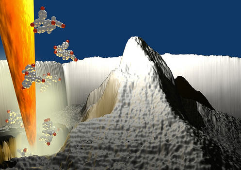
Here's a look at a 3D image of the heated nanoscale silicon tip carving out a replica of the Matterhorn, the Swiss mountain. The 25 nanometer-high 3D replica of the Matterhorn was created on molecular glass.
The map was created using "nanopatterning" with a silicon tip (right) that chisels away material from a substrate. This nanoscale tip is 10,000 times smaller than an ant, or 500 nanometers in length and a few nanometers high. IBM said that said the tip can create 2D and 3D patterns and structures as small as 20 nanometers.
Gallery: IBM's 3D nanoscale breakthrough makes the world a lot smaller
The tip is similar to the kind used in atomic force microscopes. It is attached to a bendable cantilever that controllably scans the surface of the substrate material with the accuracy of one nanometer -- a millionth of a millimeter. By applying heat and force, the nano-sized tip can carve out patterns.
The paper outlining the discovery is published in the journals Science and Advanced Materials. In the paper, IBM's research team, based in San Jose and Zurich, walk through how it created a complete 3D map 22 by 11 micrometers. How small is that? Think 1,000 world maps on a grain of salt. The 3D map is composed of 500,000 nanoscale pixels and took 2 minutes and 23 minutes to create.
Here's a look at the 3D map:
What does this breakthrough mean? IBM said that its tool can be used to create tiny machines that can repair health issues. In addition, IBM's breakthrough could affect everything from electronics manufacturing to semiconductors to medicine and life sciences to opto-electronics. Of course, nanopatterning can benefit IBM's chip and systems business in the future and applications for water purification and medical diagnostics.
A IBM spokeswoman said that IBM is in talks to license the technology to other companies and universities.
An snippet from the Science article explains the significance:
For patterning organic resists, optical and electron-beam lithography (EBL) are the most established methods, but at resolutions below 30 nanometers, inherent problems exist caused by unwanted exposure of the resist in nearby areas. We present a scanning-probe lithography method based on the local desorption of a glassy organic resist by a heatable probe. We demonstrate patterning at a half pitch down to 15 nanometers without proximity corrections and throughputs approaching those of Gaussian EBL at similar resolution. Patterns can be transferred to other substrates, and material can be removed in successive steps in order to fabricate complex three-dimensional structures.
Kick off your day with ZDNet's daily email newsletter. It's the freshest tech news and opinion, served hot. Get it.


Talkback
Bajeebers
not to mention...
And it's close enough to say ALL technology is used for evil purposes first. I see "Brave New World" in this one long before it'll be repairing anyone's 'health issues.'
Great invention
The great invention of IBM researchers who have produced a revolutionary technique to create 3D objects at the nanoscale. This is a big technological step, but also useful for society. Great article, I want to thank you for the information.
<a href="http://www.3cpromotion.com">gadget aziendali</a> .
RE: IBM breakthrough means its a nanoscale world after all
Wow.
You know what this means. The fine print on future advertising is going to get very hard to make out...
New font for ad mat
RE: IBM breakthrough means its a nanoscale world after all
AFM Guided Nanomachining which has been used for more
then TEN YEARS by semiconductor companies including
IBM to precisely shape photomasks with better then 20 nm
resolution in x,y and 5 nm resolution in z. Using diamond
probe/cutters the hardest materials known are machined
every day. Unlike this announcement which is for 2.5D or
height map surface shaping our methods can also shape
fully 3D objects. So where's the meat?
magnetic structure implications
Thermoelectric (TE) devices are solid-state devices that convert thermal energy from a temperature gradient into electrical energy (Seebeck effect) or convert electrical energy into a temperature gradient (Peltier effect).
In the quantum dynamics world, this also will have extremely important implications of harnessing the Casimir Effect that is an important issue in magnetics. For more on this subject go to wikipedia http://en.wikipedia.org/wiki/Casimir_effect
RE: IBM breakthrough means its a nanoscale world after all
Put the entire bible on a Penny
RE: IBM breakthrough means its a nanoscale world after all
Excuse me you can put the entire Bible in the eye spot of Lincoln. In fact the smaller the better and cheaper.
Problem is you can't read it and rubbing it once wipes it clean. On the other hand sell it for $10 per penny by putting the actual penny in a big jar with 100,000 other pennies- its the Christian thing to do.
RE: IBM breakthrough means its a nanoscale world after all
Access to the original scientific article
Adrian Miller
Editor, Advanced Materials
RE: IBM breakthrough means its a nanoscale world after all
The link does not work.