Exaflop computing: Moore's Law isn't dead, It's Moved to Warp Speed

Silicon Nanophotonics will usher in a completely new age of computing and power applications that we've only seen on Star Trek (image: IBM)
The universe has a funny way of playing karma tricks on us writers that follow the tech industry and dare to make sweeping prognostications about future trends.
For example, yesterday, my ZDNet Storage Bits blogging colleague Robin Harris wrote that the industry may have hit the wall in terms of increasing computing performance.
Then on the same day my employer, IBM, pulled the rug out from under him. Sorry Robin. It happens to the best of us. Seriously, I feel for you man.
The funny thing about Moore's Law is that every single time the industry calls for its inevitable demise, the Gods of Technology come and knock you on your ass. When we think we've pushed lithography and compacting transistors to their absolute limit, an advance in technology allows the trend to continue as it always has been.
This time, however, instead of just proving itself consistently correct, Moore's Law is going to have to be completely re-written -- instead of microprocessor technology doubling its performance every two years, we'll be looking forward to ten to twenty fold increases in computational power, at a bare minimum, every five years.
This increase in performance is so significant that the math itself is mind-boggling and it becomes difficult to actually relate to it in conventional terms, or even express it in a quantifiable fashion that makes sense to information technology practitioners outside of very high-end scientific research.
Today, advances in microprocessors are built on the premise of cramming as many transistors onto a piece of silicon as possible. Over the last four decades, we've continued to advance processing power by using different lithography techniques that allow semiconductorsto be manufactured in densities of continually decreasing nanometers in width.
Robin may indeed be correct that we may have hit the wall with this approach and advances using conventional microprocessor design may only result in very small incremental improvements. Eleven nanometers may be the practical limit as to how small we can go before we hit the physical limits of what can be done using current semiconductor technology.
However, what IBM showed to the public on December 1, 2010 changes the game dramatically, especially for supercomputing applications. Eventually, these advances will filter down to the enterprise systems and even consumers.

Artist's conception of the future application of photonic routing elements onto a silicon wafer (IBM)
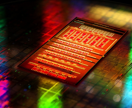
This technology -- with a name pulled seemingly right out of Star Trek is called CMOS Integrated Silicon Nanophotonics.
Without getting too intergalactic and too technical of a description of how it actually works, it is essentially the fusion of optical technology with semiconductor technology. Instead of using semiconductor pathways to route data and for the processor interconnects, light pulses are being used instead, using components called Silicon Nanoscale Photonic and Electronic Transceivers, or SNIPERS.
Next Page: The Age of Exaflops
To put all of this techno-jargon in the proper perspective, one must understand what is currently the benchmark for most powerful supercomputer in the world, the Tianhe-1A.
This powerful Chinese supercomputer has achieved 2.67 Petaflop/s or 2.67 quadrillion floating point operations, per second.
This is so amazingly fast that it realizes the kind of scientific research and advanced simulation that only 10 years ago could only exist in a computer scientist's wet dreams. But the Tianhe-1A uses strictly conventional computer technology, assembled from over 14,000 Intel Xeon 5670-series x86 processors and 7,000 nVidia Tesla GPUs using a custom high-speed interconnect network that operates at 160Gbps per second.
But compared to future nanophotonics-based systems, assessing the legacy performance of the Tianhe-1A will be like comparing the top speed of a Segway personal transport to that of a Bugatti Veyron. Or an X-15.
The first application of IBM's nanophotonics technology will be used in the Blue Waters supercomputer, which will be installed at the National Center for Supercomputing Applications (NCSA) in Urbana, Illinois in the Summer of 2011. This system, which is based on large blade clusters of IBM's 8-core POWER7 chip, will have a maximum peak throughput of 10 Petaflop/s, roughly four times faster than the Tianhe-1. It will also be much more compact and power-efficient as well, making it the most "green" supercomputer ever created.
Also Read: Super Duper Linux Computers (ZDNet Linux and Open Source)
However, even the Blue Waters supercomputer will become a clunky dinosaur once more and more nanophotonics elements are integrated onto microprocessors and replace many of the functions that traditional semiconductors perform today. And as with all supercomputing technologies, the equivalent of N minus 2 generations of processor performance will quickly find their way into enterprise systems and even consumer electronics.

Projected technological progression of photonics integration in supercomputing (IBM)
Eventually, perhaps by the year 2020 or even sooner, nanophotonic supercomputers will exist that approach the Exaflop range in terms of performance. What's an Exaflop? Well, try measuring the aggregate performance of about 250 Blue Waters or 1000 Tianhe-1A supercomputers and that's what you'll get. Did your head just explode? No? Because mine just did.
So with Exaflop-level supercomputing and enterprise computing, or even Petaflop-level consumer computing, just what exactly can you do with all of that processing power?
Well, with Exaflop/s, you can do the sort of things that take current supercomputers weeks or yearsto do in only minutes or days. It would allow the average citizen to gene sequence their babies the moment they are born to anticipate future diseases for an entire lifetime, or sequence their own DNA and apply corrective action as needed, such as synthesize custom medications.
It would allow for the real-time simulation of complex systems such as world weather and allow for meteorological science to advance at a level approaching magic or witchcraft -- the ability to accurately model how destructive storms such as tornadoes and hurricanes actually work and form, and accurately predict how they will behave.
It would permit our various government intelligence agencies, such as the National Security Agency and well as the National Reconnaissance Office to perform advanced signal intelligence (SIGINT) and space imaging in real time, determine threats to our national security and respond to it in kind with military strikes and with covert operations almost instantaneously. It would completely re-define what we understand today as rapid response and operational readiness.
The very same technology used for military applications, along with a much larger global array of radio telescopes than what we possess today, could also be used to perform much more comprehensive real-time signal spectrum analysis of extraterrestrial radio emissions and actually allow SETI to prove the existence of the E.T's we've been trying to locate for over 40 years, if those signals do indeed exist.
Beyond brute force computational applications, Exaflop and commodity Petaflop computing will almost certainly allow for the creation of intelligent robots and software agents, perhaps as brilliant as a trained circus dog, an advanced primate, a five year old child, or even more depending on advancements in computer learning.
It would allow for the real-time rendering of computer-generated imagery from today's biggest and most expensive Hollywood blockbuster films (or even better) in virtual reality or virtual worlds for the average citizen. These types of games and fully-immersive artificial realities would make the most advanced XBOX 360 or Playstation 3 first-person game look about as sophisticated as PONG.
Essentially, we're talking about the delivery of The Matrix as a commercial software product.
There are certainly other applications for commodity Petaflop and Exaflop supercomputing that people haven't even dreamed of yet. But I think we can say for sure that Moore's law hasn't run out -- instead It's been revised with a calculus that defies imagination.
What else will we do with commodity Petaflop and Exaflop computing? Talk Back and Let Me Know.
Disclaimer: The postings and opinions on this blog are my own and don’t necessarily represent IBM’s positions, strategies or opinions.