Inside IBM's 300mm chip fab: Photos

Seventy miles north of New York City, in the heart of the Hudson Valley, lies IBM's vast East Fishkill site.
Opened in 1963, the site has grown to encompass 46 buildings over 885 acres, which IBM now shares with nine other companies. Up to 6,000 IBMers work here, 1,000 of them in the site's 300mm chip fab, which opened in 2002.
The site works "to provide the server team, both z and p, early access to technology, and to work together to customise that technology," fab operations director John Arthur says. The fab also produces chips for companies such as Cisco, Microsoft, ST Ericsson, Qualcomm and Samsung, and has a sideline in producing silicon for games consoles: the chips for the Nintendo Wii U system are made here, for example.
To enter the fab floor, employees have to pass through a clean room, where they put on hair nets, latex gloves and body suits - only their eyes are left exposed. No photos are permitted inside the $6bn facility, so all pictures here are provided by IBM.
The big blue (no pun intended) machines above are stockers, which hold the wafers until they're ready to move along the line and be processed.
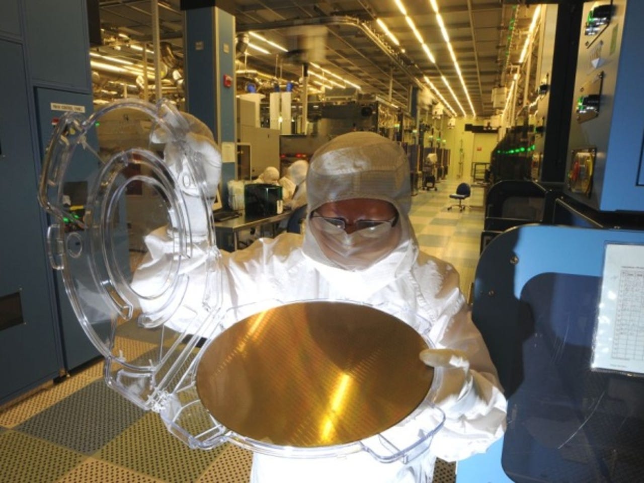
Above, IBM employee Mary Westermann inspects one of the fab's 300mm silicon wafers.
The East Fishkill fab turns out the company's 32nm Power7 chips. Such is their complexity, they require 1,200 separate steps to make, and have a yield of around 50-60 percent, according to Arthur. "The size and complexity of the chip generally dictates the yield," he explains. "A smaller chip with less function will yield higher, a more complex chip with more function will generally yield less. Some of our OEM chips have yields that are in the 90s."
Arthur is heading up the project to build the next generation of Power chips, Power8, which are still in the very early stages of design. "The chip designers use mainframes to design these things. We're building chips so we can make the machines so we can design the next generation of chips," he says.
Preventing contamination on the fab floor is paramount, hence the workers' suits. Handling of the wafers is done by cubed robots such as the one above, which move around on tracks attached to the ceiling. They ferry stacks of wafers in batches of 25 from stockers to machines where the circuitry is printed, before transferring them to other parts of the fab for quality testing. With an older chipset such as the Power7, now two years old, only about three wafers of each set of 25 are tested for imperfections, Arthur says. With a newer chip design, a higher number would be examined.
There are around 350 tool operators on the fab floor, though their job is to test and check tools rather than operate them. They are joined by nearly 500 workers employed by IBM's partners, such as Samsung, Global Foundries and ST Micro, who have access to the fab and can work on the tools supplied by their companies.
Alongside IBM Research in nearby Yorktown, much of the fab's work here is focused on developing high-performance chips.
Arthur says the fab is unusual in having production and development share the same facility. "That's rare in the industry. The plus of it is, if you work together, you can save capital equipment, because you're sharing it. The negative is, if you're sharing it, you fight about who gets it," he says, adding that balancing the needs of the two is one of the biggest challenges of his job.
The East Fishkill fab runs three shifts 24/7, and closes down for only three shifts a year: Christmas Eve, Christmas Day and Christmas Night. "We ask for volunteers. We're not at full staff but we actually run those shifts," Arthur says. "The last time this facility closed was four years go. We closed it to do some major preventative maintenance on some of the infrastructure."
During Hurricane Sandy, in October, the fab didn't lose power, but was hit instead by power spikes. "Our equipment has anywhere from seven to 20 PCs that control it," Arthur explains. "So what appears to be the weak link on the tools is the PCs. If you lose power, or if it drops a certain percent for so many cycles, the PC will just lock up. We ended up with 17 power dips here [during Sandy]. We weathered 15. Number 16 took the fab, shut the tools off." It took about eight hours for the tools to restart, he adds.
Power to the fab is fed from three directions, Arthur says, "so we can actually take a hit on one, if the other two stay up... What hurts us is if more than one goes down".
With so much automation on the fab floor, communication grew to be a problem. IBM resolved the issues by sticking a great big whiteboard in the middle of the fab (visible on the wall of the blue stocker to the left) so that workers can leave notes for the following shift. In a room where one piece of equipment can cost up to $13m, it's a startlingly low-fi touch.
While the East Fishkill fab is tooled to a 32nm process, IBM is looking at the next steps in the Moore's Law chain. "We are actually running designs in 22nm, the next generation," Arthur says. "There is 14nm in development out there and 10nm is [being developed] in Albany."
All eyes in the industry are on the shift to 450mm wafers, and the improvements in productivity that should bring. "When the next wafer size hits, you're gonna have to build a new fab, because the tools are not compatible," Arthur explains.
IBM is one of five companies in a consortium developing the tools to be used in a 450mm facility. "The investments will be mind-boggling," Arthur says. "To build one of these factories now from scratch is about $6bn for about 1,000 wafer strikes a day. This new one will be in the range of $10-12bn." 2016-17 is Arthur's prediction for when the first 450mm fab will be up and running - and he's reluctant even to commit to that.
Chip makers are already using ultraviolet photography and liquid immersion to produce chips - the other big shift on the horizon, according to IBM, will be the move to Extreme Ultraviolet (EUV) production. This is a form of what Arthur calls "very sophisticated photography" that could be used to print the next generation of chips. "The cost of those tools is staggering - numbers like a quarter of a billion dollars," he adds. "But it is what will allow you print lines that are 8nm or 6nm. That's the rub. When do the current ultraviolet tools run out of gas?"
The path ahead to the next chip process is just about visible - after that, everything is murky. But, as Arthur points out, this is nothing new: "I've been here 32 years, working on semiconductors for 28 of those, and every generation we're in, we say, we see the path to this one, and maybe, if we're lucky, the one beyond. And then we say we have no idea. So it requires invention."
All Images courtesy of IBM.