Inside Intel's 50Gbps silicon optics

Intel has debuted the prototype of a high-speed fibre optic data system based on silicon chips with integrated lasers and detectors, which it says can revolutionise affordable data communications across IT.
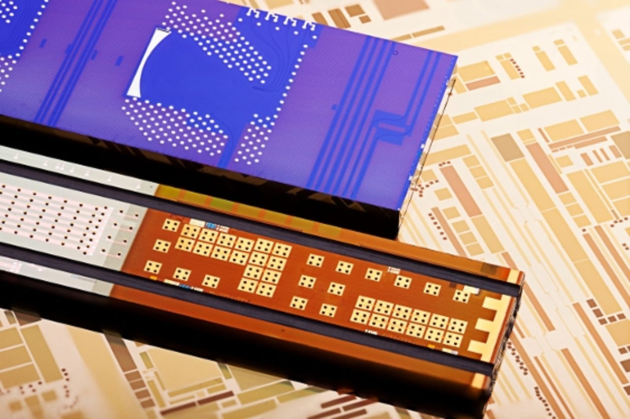
Intel's 50Gbps silicon laser transmitter, at bottom right, and optical receiver, at top left, connected by a standard fibre. The transmitter chip is the long silver device behind the connector; the smaller silver rectangle beneath it contains standard driver circuitry. Key points to note are the normal printed circuit board and construction techniques: one of Intel's key claims for this technology is that it can be manufactured and used like any other electronic component. Current optical networking components need specialist techniques of construction and use, which increases their cost and limits their usability.
For more on the technology's debut, see our
Intel shows off ultra-fast silicon optical network story. For more photos, click through to the next page.
Although there are two chips, one for receive and one for transmit, this will change. Intel is fine-tuning the very different processes needed to make the receiver and the transmitter first, and will worry about combining them onto a single chip later. In principle, though, both functions can work in a single chip, and ultimately will.
The receiver chip, at top, and the transmitter chip, outside their packaging. Both require complex and non-standard fabrication processes — and indeed have been through multiple processing stages in Intel and partner chip factories around the world. Most of the work has been done in Israel, with the laser also being constructed at the University of California at Santa Barbara. Intel is currently considering how best to set up full-scale production facilities, and where they should be.
Inside the silicon laser chip. The light itself comes from a layer of indium phosphide, much like an ordinary light emitting diode (LED). This shines down into a set of channels in the silicon beneath, forming the resonant cavities required for lasing. This is easy to mass-produce and easy to tune to different wavelengths — two essential attributes to make the technology truly mass-market.
Another essential part of a mass-market product is ease of use. Here, Intel says it has combined cheap and simple techniques to interface the fibre itself to the active components, something that normally needs expensive alignment and preparation techniques. The plug is aligned directly into grooves in the silicon die itself, using the extreme accuracy of silicon production processes to solve a mechanical problem.
Intel has two parallel paths to increasing the bandwidth of this system: adding more lasers, and making them faster. By combining both techniques, Intel says, it can take the basic ideas behind the current demonstration device and scale them directly to terabit speeds and beyond with no further major advances required.
Intel Labs fellow Mario Paniccia (right) with Professor John Bowers of the University of California at Santa Barbara, showing off the technology with the quiet yet focused satisfaction due to great inventors. Intel's collaboration with Bowers led to the development of the hybrid silicon laser at the heart of the system.
Inside the receiver chip, a demultiplexor splits the incoming light up into the different frequencies needed to feed to the parallel bank of photodetectors. The demultiplexor works exactly like a prism separating white light into rainbow components, except that it works in the infrared. Although silicon looks metallic in visible light, at infrared it is more like transparent glass — a key physical attribute that makes the whole system possible.
Inside the transmitter chip. The individual hybrid silicon lasers are given their own 12.5Gbps modulator to create four streams of pulsed light at different wavelengths, that are then combined into a single beam by a multiplexor. Each of these three stages is normally carried out by discrete components, adding enormously to the cost and complexity of the process: here, they can be manufactured in one go, and chips can be equipped with as many channels in parallel as needed.