UNSW researchers 'growing' semiconductors for smaller electronics

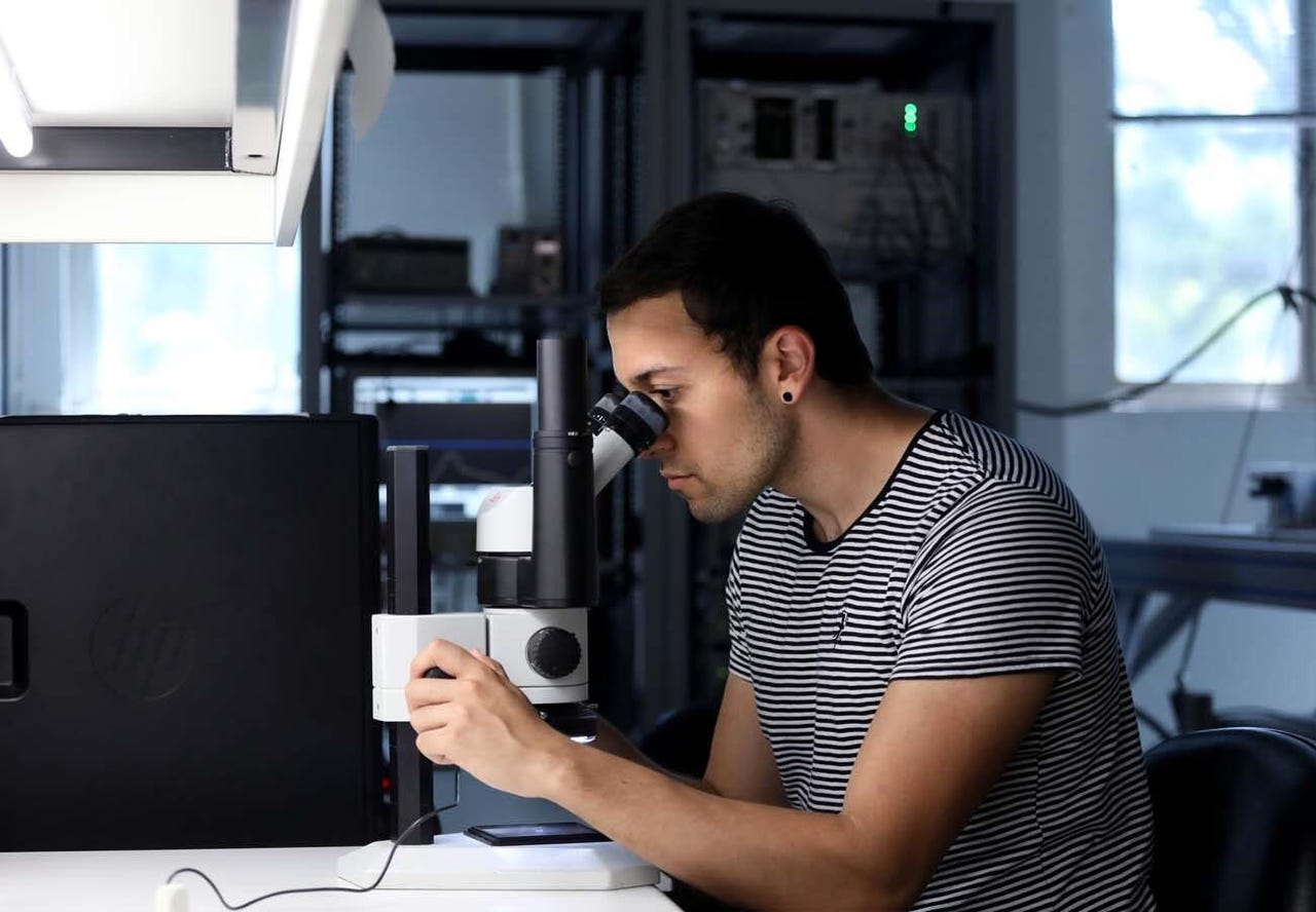
Lead author FLEET PhD student Yonatan Ashlea Alava (UNSW)
Researchers from the University of New South Wales (UNSW) have published a study they claim shows capabilities in building out "home-grown" semi-conductors for use in ultra-small electronic devices, as well as in quantum computing.
The work out of the ARC Centre of Excellence in Future Low-Energy Electronics Technologies (FLEET) said that "growing" electronic components directly onto a semiconductor block avoids messy, noisy oxidation scattering that slows and impedes electronic operation.
UNSW Professor Alex Hamilton said the home-grown, all single-crystal design would be ideal for making ultra-small electronic devices, quantum dots, and for quantum bit (qubit) applications.
"Making computers faster requires ever-smaller transistors, with these electronic components now only a handful of nanometres in size -- there are around 12 billion transistors in the postage-stamp sized central chip of modern smartphones," the researchers said.
They said in even smaller devices, however, the channel that the electrons flow through needs to be very close to the interface between the semiconductor and the metallic gate used to turn the transistor on and off.
Unavoidable surface oxidation and other surface contaminants cause unwanted scattering of electrons flowing through the channel, and also lead to instabilities and noise that are particularly problematic for quantum devices, the researchers explained.
"In the new work we create transistors in which an ultra-thin metal gate is grown as part of the semiconductor crystal, preventing problems associated with oxidation of the semiconductor surface," said Yonatan Ashlea Alava, FLEET PhD student and a lead author of the research.
"We have demonstrated that this new design dramatically reduces unwanted effects from surface imperfections, and show that nanoscale quantum point contacts exhibit significantly lower noise than devices fabricated using conventional approaches."
The researchers said one of the challenges was that electron scattering limits high-frequency components.
The mission to make increasingly smaller electronic devices demands the conducting channel in high electron-mobility transistors (HEMTs) be in close proximity to the surface of the device. The challenging part, the researchers said, has its roots in simple electron transport theory.
"When electrons travel in solids, the electrostatic force due to unavoidable impurities/charge in the environment causes the electron trajectory to deviate from the original path: The so-called 'electron scattering' process. The more scattering events, the more difficult it is for electrons to travel in the solid, and thus the lower the conductivity," they said.
"The surface of semiconductors often has high levels of unwanted charge trapped by the unsatisfied chemical bonds -- or 'dangling' bonds -- of the surface atoms. This surface charge causes scattering of electrons in the channel and reduces the device conductivity. As a consequence, when the conducting channel is brought close to the surface, the performance/conductivity of the HEMT plunges rapidly."
Additionally, they said the surface charge creates local potential fluctuations which results in charge-noise in sensitive devices such as quantum point contacts and quantum dots. It also lowers the conductivity.
The solution, the research claimed, is growing the "switching gate" first to reduce scattering.
Working with wafer growers at Cambridge University, the team at UNSW showed the problem associated with surface charge can be eliminated by growing an epitaxial aluminium gate before removing the wafer from the growth chamber.
"We confirmed the performance improvement via characterisation measurements in the lab at UNSW," co-author Dr Daisy Wang explained.
"The team compared shallow HEMTs fabricated on two wafers with nearly-identical structures and growth conditions -- one with an epitaxial aluminium gate, and a second with an ex-situ metal gate deposited on an aluminium oxide dielectric.
"They characterised the devices using low-temperature transport measurements and showed the epitaxial gate design greatly reduced surface-charge scattering, with up to 2.5x increase in conductivity."
They also showed, UNSW explained, that the epitaxial aluminium gate could be patterned to make nanostructures.
"A quantum-point contact fabricated using the proposed structure showed robust and reproducible 1D conductance quantisation, with extremely low charge noise," it added.
"The high conductivity in ultra-shallow wafers, and the compatibility of the structure with reproducible nano-device fabrication, suggests that MBE-grown aluminium gated wafers are ideal candidates for making ultra-small electronic devices, quantum dots, and for qubit applications."