Search
  • Videos
  • Windows 10
  • 5G
  • Best VPNs
  • Cloud
  • Security
  • AI
  • more
    • TR Premium
    • Working from Home
    • Innovation
    • Best Web Hosting
    • ZDNet Recommends
    • Tonya Hall Show
    • Executive Guides
    • ZDNet Academy
    • See All Topics
    • White Papers
    • Downloads
    • Reviews
    • Galleries
    • Videos
    • TechRepublic Forums
  • Newsletters
  • All Writers
    • Preferences
    • Community
    • Newsletters
    • Log Out
  • Menu
    • Videos
    • Windows 10
    • 5G
    • Best VPNs
    • Cloud
    • Security
    • AI
    • TR Premium
    • Working from Home
    • Innovation
    • Best Web Hosting
    • ZDNet Recommends
    • Tonya Hall Show
    • Executive Guides
    • ZDNet Academy
    • See All Topics
    • White Papers
    • Downloads
    • Reviews
    • Galleries
    • Videos
    • TechRepublic Forums
      • Preferences
      • Community
      • Newsletters
      • Log Out
  • us
    • Asia
    • Australia
    • Europe
    • India
    • United Kingdom
    • United States
    • ZDNet around the globe:
    • ZDNet France
    • ZDNet Germany
    • ZDNet Korea
    • ZDNet Japan

Photos: Intel's Single-chip Cloud Computer

6 of 12 NEXT PREV
  • intelscc9labout.jpg

    The Intel Germany Research Center at Braunschweig, Lower Saxony, where much of the design of the SCC took place. Other Intel labs in Bangalore and the US also contributed to the project, which the company says is a good example of how it's co-ordinating research efforts around the globe.

    Published: December 2, 2009 -- 18:00 GMT (10:00 PST)

    Photo by: Intel

    Caption by: Rupert Goodwins

  • intelscc9labin.jpg

    Inside one of the three main Braunschweig lab areas — this one is where emulation and power testing takes place. Note the curious tidying power of a PR photographer.

    Published: December 2, 2009 -- 18:00 GMT (10:00 PST)

    Photo by: Intel

    Caption by: Rupert Goodwins

  • intelscc2director.jpg

    Sebastian Steibl, head of Intel's Braunschweig lab. The centre also specialises in emulation, building high-performance hardware for the rest of Intel that lets the company test processor ideas without committing to silicon.

    Published: December 2, 2009 -- 18:00 GMT (10:00 PST)

    Photo by: Rupert Goodwins

    Caption by: Rupert Goodwins

  • intelscc3scc.jpg

    The SCC is a prototype and there is no intention of turning it into a product. However, the basic ideas it's intended to test are ones Intel hopes will provide an efficient and scalable way of building many more cores than 48 into new products. Internally, the company is looking at 256-core devices, but has no intention of stopping there.

    Intel demonstrated the SCC running a standard datacentre computing application, where multiple servers are controlled through JavaScript. The same applications could run practically unchanged on a set of discrete servers or on the chip, as the cores in the SCC look like Pentium processors to software.

    Screenshot: Intel

    Published: December 2, 2009 -- 18:00 GMT (10:00 PST)

    Caption by: Rupert Goodwins

  • intelscc1mobo.jpg

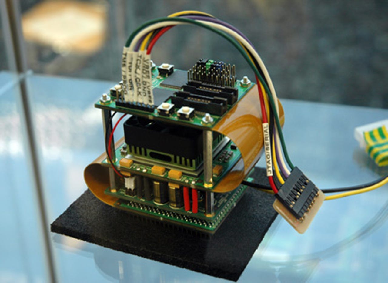
    The experimental 'Copper Ridge' motherboard will be shrunk to a standard size before systems become available to researchers. Most of the complexity on this prototype is for signal monitoring and the highly configurable multi-voltage power management system.

    Published: December 2, 2009 -- 18:00 GMT (10:00 PST)

    Photo by: Rupert Goodwins

    Caption by: Rupert Goodwins

  • intelscc8broken.jpg

    The Brockentower, a speciality of the Braunschweig labs. This is a software-reconfigurable processor that can be set up very quickly to test out new architectures. When it was pointed out to a researcher that, if this was sold as a product, no customer would ever need to buy a new processor again, the engineer fell silent and then changed the subject.

    Published: December 2, 2009 -- 18:00 GMT (10:00 PST)

    Photo by: Rupert Goodwins

    Caption by: Rupert Goodwins

  • intelscc4fractal.jpg

    Fractal generation is a classic test for multiprocessing, as the mathematics across the image can be run in parallel during each iteration of the function. Here, the SCC is generating fractals in conjunction with an Intel multiprocessing control and monitoring program, showing that standard development and management tools are easily coupled to the hardware.

    Published: December 2, 2009 -- 18:00 GMT (10:00 PST)

    Photo by: Rupert Goodwins

    Caption by: Rupert Goodwins

  • intelscc5corecomms.jpg

    On this screen, the top red and blue line is one core controlling others displayed beneath it. As each core completes its task, its bar changes colour and it communicates the fact back to the manager.

    Published: December 2, 2009 -- 18:00 GMT (10:00 PST)

    Photo by: Rupert Goodwins

    Caption by: Rupert Goodwins

  • intelscc6power.jpg

    After running the fractal test, the chip consumes 55 watts in idle mode. This could be dialled down lower, but is only around a watt per core. Intel hasn't said how fast each chip runs, but one characteristic of multicore systems is that when running undemanding tasks they can prove very power efficient indeed.

    Published: December 2, 2009 -- 18:00 GMT (10:00 PST)

    Photo by: Rupert Goodwins

    Caption by: Rupert Goodwins

  • intelscc7cpu.jpg

    The SCC chip next to a 2-Euro coin (for UK readers, that's roughly the size of a one-pound coin). Although large by modern die standards, the chip is being made in very small numbers — hundreds or thousands — and thus a handful of wafers will constitute a full production run.

    Published: December 2, 2009 -- 18:00 GMT (10:00 PST)

    Photo by: Rupert Goodwins

    Caption by: Rupert Goodwins

  • intelscc10wafer.jpg

    The 48 cores can be seen, mostly configured as dual-core areas of the die, with the 6x4 networking layout also clearly visible.

    Published: December 2, 2009 -- 18:00 GMT (10:00 PST)

    Photo by: Intel

    Caption by: Rupert Goodwins

  • intelscc11scc2.jpg

    The configuration both of the chip itself and the dual-core basic computational unit within it. The message buffer and router are key to the chip's unique characteristics, corresponding roughly to a very fast network linking discrete servers in a datacentre.

    Screenshot: Intel

    Published: December 2, 2009 -- 18:00 GMT (10:00 PST)

    Caption by: Rupert Goodwins

6 of 12 NEXT PREV
Rupert Goodwins

By Rupert Goodwins | December 2, 2009 -- 18:00 GMT (10:00 PST) | Topic: Servers

  • intelscc9labout.jpg
  • intelscc9labin.jpg
  • intelscc2director.jpg
  • intelscc3scc.jpg
  • intelscc1mobo.jpg
  • intelscc8broken.jpg
  • intelscc4fractal.jpg
  • intelscc5corecomms.jpg
  • intelscc6power.jpg
  • intelscc7cpu.jpg
  • intelscc10wafer.jpg
  • intelscc11scc2.jpg

Intel's experimental 48-core SCC processor is a pointer to the future says the company. Check out the chip and the lab where it was conceived in our gallery.

Read More Read Less

The Brockentower, a speciality of the Braunschweig labs. This is a software-reconfigurable processor that can be set up very quickly to test out new architectures. When it was pointed out to a researcher that, if this was sold as a product, no customer would ever need to buy a new processor again, the engineer fell silent and then changed the subject.

Published: December 2, 2009 -- 18:00 GMT (10:00 PST)

Caption by: Rupert Goodwins

6 of 12 NEXT PREV

Related Topics:

Hardware Reviews Storage Data Centers
Rupert Goodwins

By Rupert Goodwins | December 2, 2009 -- 18:00 GMT (10:00 PST) | Topic: Servers

Show Comments
LOG IN TO COMMENT
  • My Profile
  • Log Out
| Community Guidelines

Join Discussion

Add Your Comment
Add Your Comment

Related Galleries

  • 1 of 3
  • AI, blockchain, servers, smartphones and more: Research round-up

    We summarise the charts that tell the tech story of the past month.

  • Windows Server vNext Technical Preview: Screenshots

    The next version of Windows Server is at an early stage of development, but some of the new functionality for orchestrating virtualised compute, storage and networking resources ...

  • In pictures: Take a look inside Telefonica's Madrid datacenter

    The Spanish telco's largest facility is based outside the Spanish capital. ZDNet was invited along to see inside.

  • Microservers: In pictures

    Tower, rack and blade servers are familiar enough, but what do microservers look like? We examine examples from HP, SeaMicro and Dell.

  • The tech behind the Bathurst 1000

    Each year, the V8 Supercars series converges on Mount Panorama for the endurance race known as the Bathurst 1000. ZDNet took a look at the tech behind the data used by the Symantec Nissan ...

  • Inside IBM's 300mm chip fab: Photos

    IBM's 300mm chip fab in upstate New York turns out high-performance chips around the clock. ZDNet was invited to take a look inside, and learn about what the future holds for chip making. ...

  • Cool runnings: IBM's recipe for a happy datacentre, in pictures

    How do you make your datacentre run better, and save money? At IBM's research labs and facilities in upstate New York, three ideas are uppermost on people's minds: energy efficiency, ...

ZDNet
Connect with us

© 2021 ZDNET, A RED VENTURES COMPANY. ALL RIGHTS RESERVED. Privacy Policy | Cookie Settings | Advertise | Terms of Use

  • Topics
  • Galleries
  • Videos
  • Sponsored Narratives
  • Do Not Sell My Information
  • About ZDNet
  • Meet The Team
  • All Authors
  • RSS Feeds
  • Site Map
  • Reprint Policy
  • Manage | Log Out
  • Join | Log In
  • Membership
  • Newsletters
  • Site Assistance
  • ZDNet Academy
  • TechRepublic Forums