Inside Intel's Pentium M/Centrino

With the launch of Intel's Pentium M/Centrino technology, the company is putting its silicon where its mouth is. Intel has long said both that the notebook market will be one of the major growth areas in the future, and that performance need not be sacrificed for portability and battery life. Unusually, the chip giant has been quite open prior to launch about the technical details of the project codenamed Banias (the major redesign of the Pentium for the portable market), and our initial tests suggest that Intel's promises about performance and battery life appear to have been kept.
Banias is now called the Pentium M, while the chipsets formerly codenamed Odem and Montara-GM are now the 855PM and 855GM respectively. The wireless side is handled by Intel's PRO/Wireless 2100 Network Connection Mini-PCI card (11Mbps 802.11b now, with faster 54Mbps variants to follow). The whole family is called Centrino, and while manufacturers are free to take individual parts, they can only get the approved logo (the one that looks like a set of dart flights) if they use a complete set.
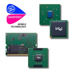
Intel's Centrino family comprises the Pentium M processor, the 855 chipset and a PRO/Wireless 2100 Network Connection Mini-PCI card. A notebook vendor can only use the logo (above) if a system uses all of these Intel components.
Pentium M architecture
The Pentium M will be available initially from 1.3 to 1.6GHz speeds, with low and ultra-low voltage variants at 1.1 and 0.9GHz emerging later. Those are maximum speeds: like previous Intel mobile processors, they're designed to run at slower rates to save battery life. One of the Pentium M's innovations is that different components within the processor chip can effectively shut down altogether when not in use, even during a single clock cycle. Intel says that most of the processor is, in fact, turned off most of the time.
The same is true of the Pentium M's very large Level 2 cache, where most of its 1 megabyte is kept in a state as close to unpowered as possible. It has dedicated circuits that keep track of recent accesses, working out how much of the circuitry can be stood down. When applications or the operating system use data from a small section of memory, the entire cache can be disabled on the fly and the data produced from a small, dedicated part of the chip -- effectively a sub-cache.
Lots of power is normally wasted doing pre-fetch and branch prediction -- two high-performance mechanisms where a processor gets information in from memory ahead of time whether it's going to be needed or not. Intel has analysed billions of lines of existing code to make the best guess as to when these mechanisms are needed, so reducing wasted memory accesses. Normal processors can waste up to 30 percent of their time recovering from mistaken predictions: the Pentium M has what Intel calls the 'best-in-class' branch prediction, with many independent circuits checking their areas of expertise and combining to produce a best guess that's around 20 percent more efficient than previous efforts.
Another standard part of processor architecture is the stack -- an area of memory that contains temporary data and memory address information. It's used intensively by all software, but the instructions that manage the stack have to go through the same processing as any others. The Pentium M spots these instructions and very early on hands them over to a special hardware unit dedicated to stack management. Intel says that this removes around 5 percent of the load on the rest of the processor.
Likewise, the Pentium M reduces processor load by combining different aspects of the program flow into single internal operations, a process called 'micro-op fusion'. Thus, multiple instructions look like single operations for most of their life within the processor, only being split up into their independent bits just before actually being executed. This creates a further 10 percent reduction in the amount of time the chip spends processing operations.
All of the above not only reduce power consumption but helps efficient processing, says Intel, and our tests bear this out -- a 1.6GHz Pentium M outperforms a 2.4 GHz Pentium 4M while delivering around 50 percent longer battery life. At full tilt, the 1.6GHz part takes 24 watts; in its most severe power saving mode it runs at 600MHz and consumes just 6 watts. The ultra-lower voltage variants are expected to manage on around half a watt at the full-blown economy setting. Manufacturers can take this advantage either as extra battery life with the same size and weight of machine as before, or keep the same battery life and make their notebooks smaller and lighter.
This graph summarises the performance and battery life advances made by the new Pentium M/Centrino notebooks. The previous generation of Mobile Pentium 4-M notebooks (green dots) were good performers (30-50 on Business Winstone 2001), but typically delivered between 2 and 3 hours' battery life. Older Mobile Pentium III-M systems (blue triangles) could exceed 3 hours' battery life, but performance was lower (20-40 on Business Winstone 2001). The three new Pentium M notebooks (pink diamonds) we have tested so far occupy the hitherto-elusive top-right quadrant of the graph, where performance is excellent (>50 on Business Winstone 2001) and battery life long (3-5 hours).
855 chipsets
The 855 chipsets also have numerous power saving tweaks, driving LCDs much more effectively and monitoring the power requirements of different system components, reducing power where possible. They are very similar, with the 855PM supporting off-chip graphics via a power-managed AGP 4X bus and the 855GM having on-chip support for LVDS output, CRT and two DVO ports. Otherwise, both chips have the same features, including a memory controller for up to 2GB of 200MHz or 266MHz DDR DRAM, in four banks, and -- of course -- extensive power management. Both chips talk to a further Intel chip, the ICH4-M, which handles input/output.
The ICH-4M has a built-in 10/100Mbps Ethernet controller, a 33MHz PCI interface, AC 97 v 2.3 for audio and modem, USB 2.0, and the Low Pincount Bus (LPB) for serial support and security token interfacing. Intel's reference design for Centrino systems expects the PCI bus to be used for its 1000MT Gigabit Ethernet product -- and the company would prefer designers to do that rather than use the ICH-4M's built-in slower Ethernet. Intel also expects the PCI bus to support CardBus and Mini-PCI, with CardBus being used for GPRS or GSM interfaces and Mini-PCI connecting to the wireless LAN solution, which is codenamed Calexico. The first wave of Centrino systems only offer 11Mbps 802.11b via a Philips Wi-Fi chip, but Intel's forthcoming wireless silicon will support 54Mbps 802.11a as well. Calexico also includes diversity reception, where it chooses the best antenna out of two for a connection depending on signal strength, and reduces interference from other devices on 2.4GHz and 5GHz via integrated narrow-band filters. An 802.11g version and a tri-standard (a/b/g) variant are expected later this year.
Intel is pushing its Wireless Coexistence Solution for Centrino notebooks, which reduces or removes interference between 802.11b and Bluetooth in the same system. This involves being careful about placing antennas and understanding their mathematical relationship, and includes some hardware and software additions in both the 802.11b and Bluetooth components.