'NanoPen' to write a new chapter in nanotech manufacturing

Among the top challenges facing the commercialization of nanotechnology is to produce a high volume of nano-scale components cheaply and efficiently. To help meet the challenge, UC Berkeley researchers are reporting the development of a "NanoPen" that could provide a quick, convenient way of laying down patterns of nanoparticles — from wires to circuits — for making tiny electronic devices, medical diagnostic tests, and other nanotech applications.
In a report published in ACS' Nano Letters, Ming Wu and his colleagues point out that there are already several different methods for producing patterns of nanoparticles (1/50,000th the width of a human hair), but those techniques tend to be too complex and slow. One such printing technique is called optical lithography, but it is already reaching its physical limits.
The researchers say that such techniques require bulky instrumentation and take minutes or even hours to complete. And they require the use of very high temperatures to apply the nanostructures to their target surfaces. These limitations prevent widespread application of such techniques, says Wu.
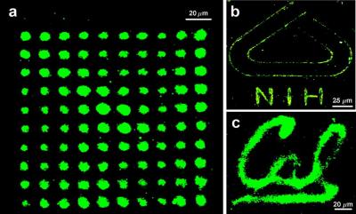
The NanoPen solves these problems, according to the research team. In lab studies, they used it to deposit various nanoparticles into specific patterns in the presence of relatively low light and temperature intensities. Below are some examples, highly magnified:
The process requires the use of special "photoconductive" surfaces, and takes only seconds to complete. According to the researchers, manufacturers can adjust the size and density of the patterns by adjusting the voltage, light intensity, and exposure time applied during the process.
