Samsung, Micron use 3D to push flash further

Flash memory has enjoyed a great run. Micron, Samsung, SK Hynix and Toshiba (SanDisk) are all manufacturing 15nm or 16nm chips that squeeze 16GB into an area about one-third the size of a penny. As costs have come down, these flash chips found their way into everything smartphones to laptop solid-state drives to servers and storage arrays.
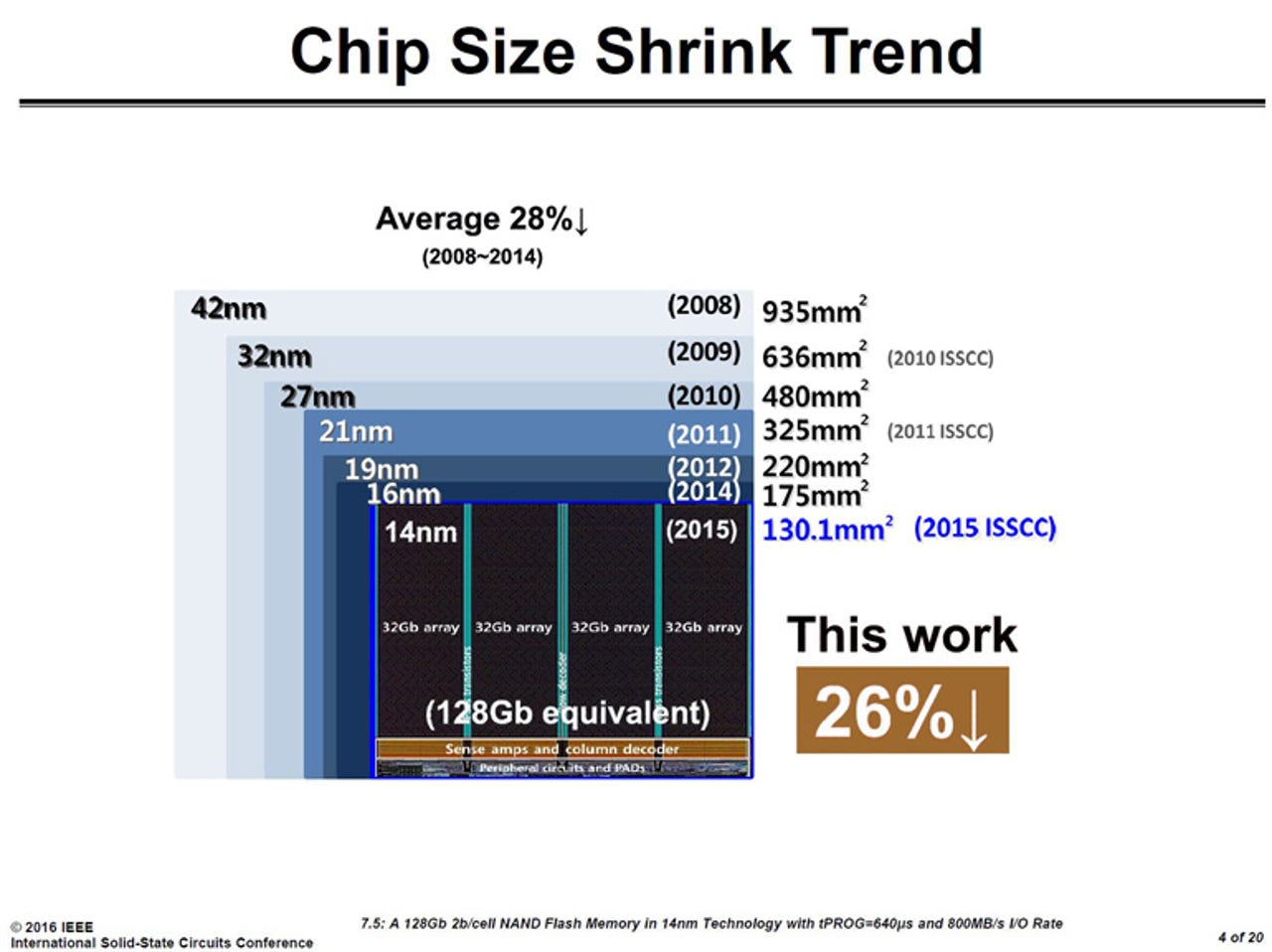
But conventional flash memory is clearly reaching the end of the road. This week at ISSCC, an annual semiconductor conference in San Francisco, Samsung talked about the difficulty of scaling planar NAND flash. The company announced a 14nm 128Gb MLC (two bits per cell) chip, but noted it wasn't able to shrink the individual memory cell much (13 percent versus the recent historical average of around 32 percent per generation). As a result, Samsung had to employ all sorts of tricks to shrink the chip around 26 percent resulting in a die size of 130 square millimeters.
Fortunately, there's an alternative. Rather than trying to shrink in two dimensions, 3D NAND uses larger memory cells stacked in multiple layers to reach higher densities in the same footprint. Think of it like building multi-story apartment buildings in cities in order to fit more people into the same space.
For now, Samsung has the lead here with what it refers to as V-NAND (Vertical NAND). The company started mass production of the industry's first 3D NAND, a 24-layer 128Gb MLC chip, in August 2013. At ISSCC 2014, the company revealed that this first-generation V-NAND with 24 layers had a die size of 133 square millimeters resulting in an areal density of 0.62 terabits per square inch. The following year, Samsung was back at ISSCC with a 32-layer 128Gb TLC (three bits per cell) device, which at just 68.9 square millimeters, has 1.19TB per square inch, surpassing the areal density of the most advanced hard drives for the first time.
This week Samsung detailed its third-generation V-NAND, a 48-layer 256Gb TLC chip measuring 97.6 square millimeters. That pushes the areal density to 1.69Tb per square inch. Most of the presentation dealt with the techniques that Samsung is using to maintain the performance and reliability of its 3D NAND as it adds more layers and makes those layers thinner (3D NAND works around some of the problems with scaling planar NAND, but it poses plenty of manufacturing challenges of its own). The company has previously said it will use this 256Gb TLC chip to make 2.5-inch SSDs with up to 16TB of storage.
The rest of the industry is now scrambling to catch up. Micron is currently producing 32-layer 256Gb MLC and 384Gb TLC chips. This week at ISSCC it revealed details of a TLC chip under development with more than 32 layers that will reach an impressive 768Gb. The company explained why, despite the use of technologies such as air gaps and thin floating gates, planar scaling has run out of steam around 16nm because the gates are packed so close together that it causes unwanted capacitance (coupling) and the number of electrons stored has dwindled, making operation less reliable.
The shift to 3D drastically reduces this capacitive coupling and restores the number of electrons stored in each cell to the equivalent of around 40nm planar flash. But it is much denser. With a die size of 179.2 square millimeters, Micron's 768Gb TLC chips has an areal density of 4.29Gb per square millimeter. In comparison, Micron's 16nm 128Gb MLC chip, has a density of 0.87Gb per square millimeter. The 768Gb chip is also equivalent to 2.77Tb per square inch--to put in in the terms used by Samsung and the hard drive industry--making it notably denser than even Samsung's third-generation 48-layer TLC chip.
Toshiba and SanDisk have announced a 48-layer 128Gb MLC and 256Gb TLC chips, which will be manufactured at the company's new Fab 2 in southern Japan starting this year (this week the company said it plans to build another 3D NAND fab next door). SK Hynix started limited production of a 36-layer 128Gb MLC chip last year, and plans to shift to a 48-layer 256Gb TLC device sometime in 2016. Most manufacturers agree that there is a relatively clear path to scale 3D NAND to around 96 layers, delivering 1Tb or more on a single chip.