Sandy Bridge: Intel's next-generation CPU

On 13 September at the Intel Developer Forum in San Francisco, Intel unveiled Sandy Bridge, the first major redesign of the x86 architecture on 32 nanometres (nm). In a series of announcements, the company described the architecture and innovations of the chip, and said that the first products will be available in 2011.
Tock follows tick
Intel's roadmap works on the 'tick-tock' model: a new manufacturing process is brought in using the existing CPU architecture ('tick'), and then a new architecture is introduced on the current manufacturing process ('tock'). The current Nehalem architecture (a tock) was introduced in November 2008, on a 45-nanometer (nm) manufacturing process. It reached the mass market in early 2010 with the 32nm dual-core Arrandale and Clarkdale (Core i3, i5, and i7) processors (a tick). These belong to the Westmere family, which also brought small improvements such as hardware-accelerated AES encryption to the Nehalem architecure. The gap since the previous Penryn (Core 2 Duo) architecture was therefore over one-and-a-half years.
Intel now has an established a 32nm manufacturing process as well as sufficient production capacity. Everything is in place for a rapid transition. In addition, smaller die sizes should result in lower production costs.
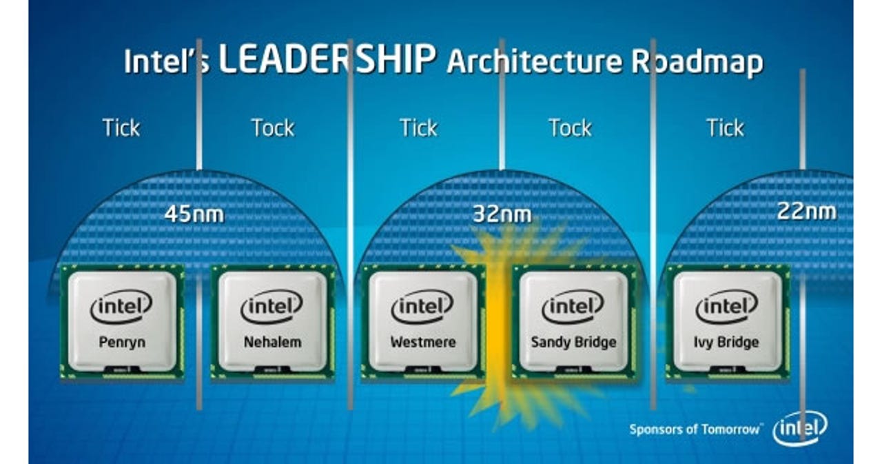
The current Nehalem microarchitecture was introduced in late 2008 in the high-end sector. One and a half years later it reached the mainstream sector with the 32nm Westmere processors (today's dual-core Core i3/i5/i7 chips)
What innovations are in Sandy Bridge?
Sandy Bridge is the first new CPU architecture from Intel since the introduction of Nehalem in November 2008. All resources such as CPU and graphics cores are connected via a ring bus with over 1,000 separate on-chip wires. This can run at 96Gbps with a 3GHz clock and is very easy to reconfigure when designing chips with different combinations of cores. According to Intel, this allows a relatively easy adjustment for different target markets: multi-cores for servers or more video units for desktops, for example.
The Hyper-Threading system introduced with Nehalem, which makes a physical core into two virtual cores by doubling the register sets, is still in use. But Intel has refined Turbo Boost by allowing all cores to overclock simultaneously for ten to twenty seconds if the chip was previously running cool. This effectively uses the chip's substrate itself as a heatsink, and requires the BIOS to know details of just how fast the cooling system can dissipate heat. OEMs are expected to configure this part of the system at design time.
Intel has also accelerated its previously unremarkable graphics technology, and says that Sandy Bridge's integrated graphics will offer the performance of entry-level GPUs. However, it will only support DirectX 10; DirectX 11 is planned for Sandy Bridge's successor, Ivy Bridge. In fact, Intel says that only tessellation is missing from the current chip, which would otherwise be able to support the new standard.
Sandy Bridge also has the SSE successor, AVX (Advanced Vector eXtensions). AVX increases the vector width from 128 bits to 256 bits. Intel promises that this will result in a doubling of floating-point performance, which will mostly benefit video processing.
Arrandale and Clarkdale had separate CPU and graphics dies bonded together in a single package. Because Sandy Bridge's graphics unit is fully integrated on the ring bus, and also shares the top-level cache with the processing cores, performance is greatly enhanced. There's also AES New Instructions (AESNI), which use a hardware encryption acceleration unit.
Westmere had the CPU core and graphics unit on the same package, but separate; Sandy Bridge puts both on the same die
How will Sandy Bridge be marketed?
Intel's current brand strategy is not particularly clear. For example, both the 1.06GHz Ultra-Low-Voltage dual-core and the 3.33GHz six-core are marketed under the same name, Core i7, despite being as far apart as the market will bear. Differentiation is only possible using the model numbers, which in this case are Core i7 620UM and Core i7-970 respectively.
The bad news is that the new Sandy Bridge processors will retain the Core i3, i5 and i7 branding: the only hint that there's a new underlying architecture will be a redesigned logo and new model numbers.
Sandy Bridge processors will use the existing Core i3, i5 and i7 branding, with just a new logo and model numbers
What is the model range?
Intel has not yet published details of the range of chips it will launch with the new architecture, but is expected to kick off with desktop chips ranging from a 2.5GHz low-power dual-core Core i3 to a 3.4GHz quad-core Core i7. Notebook processors will include dual-core models from a 2.5GHz Core i5 to a 2.7GHz Core i7, and quad-core Core i7s running between 2.2GHz and 2.5GHz.
What performance boost can be expected?
Christmas is coming before Sandy Bridge, so Intel is keen not to spoil the sales of existing notebooks and isn't telling anyone just how fast Sandy Bridge will be when it arrives early in 2011.
However, some applications were shown off at the Intel Developer Forum (IDF) that allow us to reach some tentative conclusions on performance: transcoding a three-minute 640-by-360 video clip took only 15 seconds on Sandy Bridge, compared to 44 seconds on a Core i5. This improvement is due to Sandy Bridge's integrated video encoding unit — the demo used a specially adapted version of CyberLink MediaEspresso. Intel is currently talking to 30 software companies about this.
Significant improvements in the integrated graphics unit were also visible at IDF: for example, the strategy game Starcraft II: Wings of Liberty ran equally well as on a similar machine with a discrete Nvidia GeForce 310M GPU. This was not possible using the HD Graphics on Arrandale or Clarkdale processors. Bear in mind, though, that the GeForce 310M GPU is an entry-level graphics chip; if you need high-quality graphics, you'll probably still need a discrete, and expensive, GPU.
When will Sandy Bridge appear in servers?
Intel will introduce server chips based on Sandy Bridge during 2011. The company has also said that Ivy Bridge, the 22nm 'tick' version of Sandy Bridge, is expected by the end of 2012.
Intel's Xeon server CPUs will be based on Sandy Bridge in the future, but the change will be gradual. Ivy Bridge is the 22nm version of Sandy Bridge
Sandy Bridge's new socket
Intel's current Core ix processors use either Socket LGA 1366 (triple-channel memory access) or Socket LGA 1156 (dual-channel). Sandy Bridge introduces yet another new socket, LGA 1155, with one fewer pin than before.
It will not be possible to equip existing motherboards with Sandy Bridge: new designs will be needed. Intel says the new architecture is just too different to make compatibility worth maintaining, but claims that the increase in performance is worth it.
Will the new chipsets support USB 3.0?
New chipsets will be needed, as well as new sockets. Although the new Sandy Bridge chipsets have not yet been officially introduced, it's already clear that they will lack USB 3.0 support. This is unfortunate because the technology has definite benefits.
PC makers will have to rely on third-party solutions at extra cost to provide USB 3.0, at least initially. Whether this will be the case for all Sandy Bridge chipsets remains to be seen.
Additional material by Rupert Goodwins, ZDNet UK