IBM Research creates 2nm test chip, eyes performance, power boost

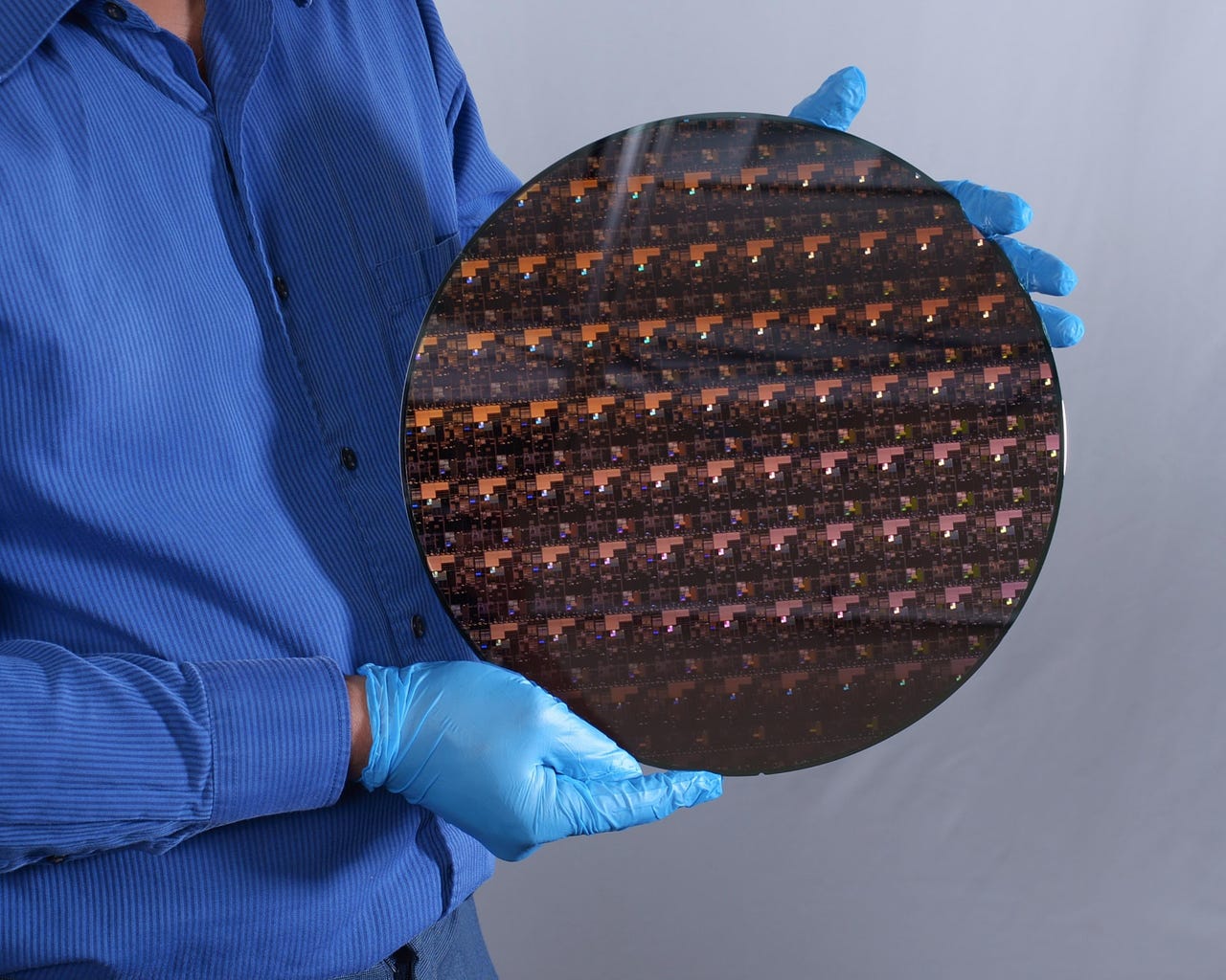
A 2 nm wafer fabricated at IBM Research's Albany facility. Credit: IBM Research.
IBM Research said it has created the first test semiconductor with 2 nanometer technology in a move that will result in a smaller energy footprint.
According to IBM, the 2nm processor will improve performance by 45% using the same amount of power or use 75% less energy while maintaining as 7nm-based chips. The test chip can fit 50 billion transistors on a chip the size of a fingernail.
IBM Research developed the 2nm test chip in its Albany, NY lab. IBM's VP of hybrid cloud Mukesh Khare said IBM produced the 2nm technology milestone on a 300mm silicon wafer built at the Albany facility.
IBM is partnered with the State of New York, Samsung Electronics and Intel on advancing semiconductor designs. IBM created the first 7nm and 5nm test chip in 2015 and 2017, respectively.
Semiconductor innovation is a hot topic in the US as the intellectual property race heats up with China. In addition, semiconductor shortages are hampering the supply chain and manufacturing in key markets.
Recent headlines include:
- Semiconductor restraints will shake up auto maker supply chains: Nvidia CEO
- Intel to invest $3.5B to expand manufacturing in New Mexico
- SK Hynix to increase spending on fab equipment in light of chip shortage
- Cisco boss expects global chip shortage to continue another six months
- TSMC sees chip constraints through 2022, will spend $100bn on boosting capacity
According to IBM, the 2nm processors will be able to accelerate applications in artificial intelligence, edge computing, autonomous system as well as other areas. IBM said it will use the technology in its IBM Power Systems and IBM Z as well as other systems.
Dario Gil, director of IBM Research, said the new processor can address sustainability and climate change. Data centers account for 1% of global energy use.
The 2nm technology will go into production toward the end of 2024, Khare said.
More: