IEDM 2017: AMD says Epyc is just the beginning

Moore's Law is slowing down and the bag of tricks that the industry uses to squeeze more out of each new generation of chips is reaching diminishing returns. It takes a lot more effort to stay on the leading edge, and it costs a lot more, eroding the economic benefits and forcing the industry to seek new solutions.
In her opening talk at IEDM 2017, an annual chip conference stretching back 63 years, AMD CEO Lisa Su talked about these challenges and her company's approach using a multi-chip architecture to "break the constraints of Moore's Law." The keynote capped a big year for AMD which shipped a long-awaited redesign of its desktop, server and mobile processors making it competitive once again with Intel in high-performance computing.
It was also a homecoming of sorts for Su, who won IEDM's student prize as an MIT grad student in 1992. She noted that a Cray supercomputer from that year--one of the fastest in the world at the time--was capable of 15 billion operations per second while this year's crop of game consoles delivers five to six trillion operations per second for around $500. "We have made tremendous progress," Su said. "But you can see that we also have the opportunity to go much further."
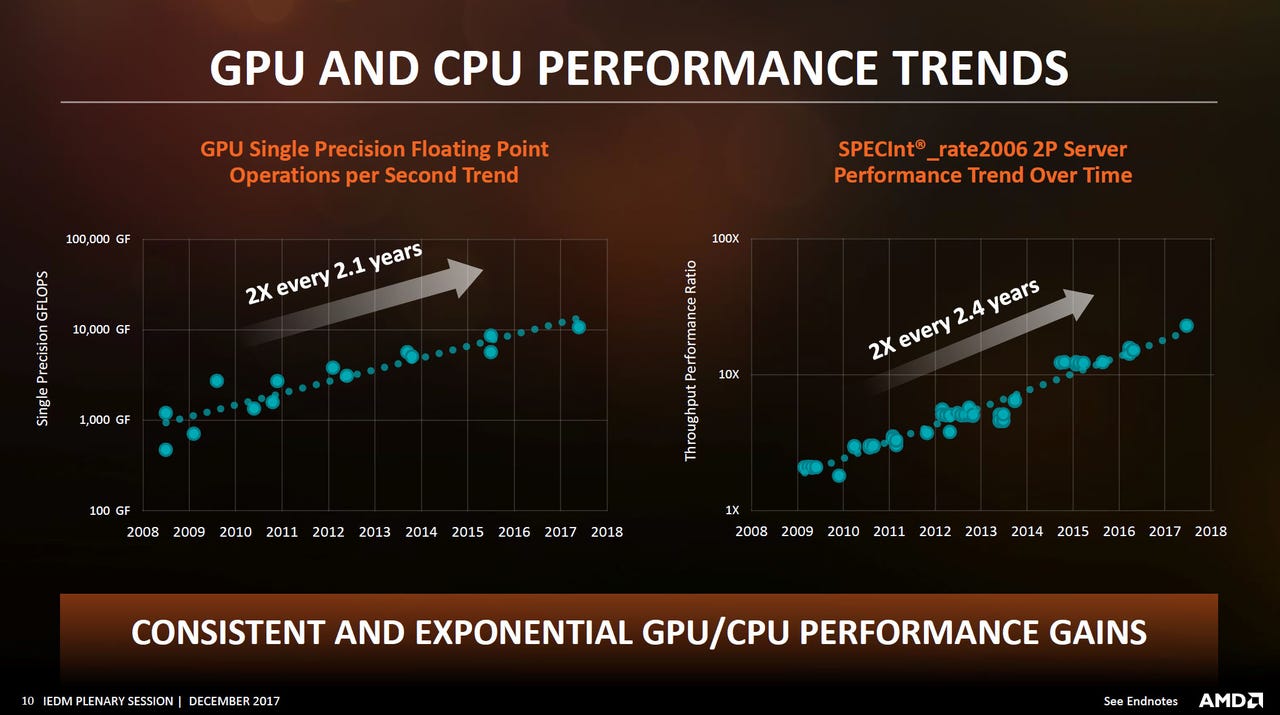
The PC may be in decline and the smartphone market is showing signs of saturation, but AMD believes a new era of immersive computing that will require a lot of computing horsepower. CPU and GPUs have been the building blocks of high-performance computing. Over the last decade, performance has doubled every 2.4 years for CPUs and every 2.1 years for GPUs, according to AMD's data. The efficiency (or performance per watt) in server chips has also doubled every 2.4 years.
But it hasn't been easy and interestingly AMD says only around 40 percent of these gains have been coming from technology shrinks. Much of the rest comes from systems and architecture design. This includes integration of more features, microarchitectural innovations, enhanced power management, and software such as better compilers. The new Zen microarchitecture, for example, increased instructions per clock by 52 percent and each Epyc 8-core die has thousands of sensors to optimize power, improving performance per watt by almost 50 percent.
For now, these tricks are continuing to deliver solid gains, but about 20 percent of it is coming from increasing overall power and die size. For example, high-end GPUs have gone from 200 watts to 300 watts as the industry gets better at dissipating heat. In a typical server chip, only a third of the power is now going directly to computation as other components such as I/O, caches and on-chip fabrics consume more power. High-performance chips now measure 500 to 600 square millimeters and some are approaching the limits of manufacturing tools (the reticle limit), most notably Nvidia's massive Tesla V100 GPU. Not surprisingly, all of this is getting very expensive and AMD showed a chart indicating that a 7nm chip will be more than twice the cost of its current 14nnm processors. Finally, memory bandwidth hasn't been able to keep up with the increased performance of CPUs and GPUs.
All of this is what led AMD to shift to a multi-chip architecture for Epyc. The flagship 32-core server chip actually consists of four 8-core 'chiplets' on an organic interposer connected with a proprietary Infinity Fabric using high-speed SerDes links. The overall die area is a bit larger due to peripheral circuitry--a total of 852 square millimeters versus 777 square millimeters for a hypothetical monolithic die--but the yield is so much higher that it costs 40 percent less. It also provides flexibility to design different products. AMD and others are also using 3D stacked DRAM known as high-bandwidth memory (HBM) to increase bandwidth, reduce power, and lower the overall footprint and complexity of designs--albeit at a cost since HBM carries a hefty premium and DRAM prices have been on the rise.
The ultimate goal is to stack not only DRAM, but also non-volatile memory, GPUs and other components directly on top of processors, Su said. Separately, Sony gave a presentation describing how it is already doing something similar for its CMOS image sensors--stacking the pixel sensor on top of 1Gb of DRAM, which is in turn stacked on top of an image processor--but there is still a lot of work to do to make extend this to high-performance computing, most notably with fabricating higher density interconnects, known as through-silicon-vias (TSVs), and dissipating all the heat trapped in that sandwich. But Su said she's confident all these issues were surmountable. The real issues, she said, are making 3D integration economical and updating the software to fully utilize these kinds of devices.
In the legacy world, "the CPU was the center of everything with other chips hanging off of it," Su said. But workloads have changed, in particular with the rise of deep learning, and there is now a lot of debate within the industry about whether the CPU, GPU, FPGAs or custom ASICs will become the primary compute element. "From my perspective, it is all of the above," Su said. "You are going to find that the world is a heterogeneous place." This will also place more importance on the interconnects that tie all of these elements together (AMD is a member of both the CCIX and Gen-Z consortiums developing this technology).
The combination of continued scaling and these techniques will continue to deliver at least a doubling of performance every 2.4 years, according to AMD. "We absolutely believe the performance gains we've seen in the last decade, we can achieve or superseded in the next decade," Su said.