AMD explains the technology behind its smaller, faster GPUs

Chipmaker AMD has announced a new graphics processor designed to show how its novel stacked memory technology can squeeze high-end gaming into much smaller, less power-hungry systems. The Radeon R9 Nano was expected--the company said a smaller board was in the works when it announced the Radeon R9 Fury family earlier this summer--but this week AMD made it official and provided the details.
Despite its small size, the Nano is very similar to its big brother. Like the flagship R9 Fury X, the Nano is based on the 28nm Fiji GPU with 64 compute units (a total of 4,096 stream processors) surrounded by 4GB of stacked DRAM with 512GB per second of peak bandwidth. The difference is that the Nano is even smaller and draws only 175 watts of power, which means it can fit in the smallest PCs. It's too early to tell exactly how this will impact performance--for that we'll need to wait for review units closer to the September 10 release date--but AMD claims it will be 30 percent faster than its previous high-end, full-size card, the R9 290X based on the 28nm Hawaii GPU, and it should run circles around other small GPUs.
What's more interesting is how AMD is packing this level of performance into such a small package without the benefit of more advanced process technology (GPUs have been stuck at 28nm for some five years now). Earlier this week, at the annual Hot Chips conference, Joe Macri, an AMD fellow and Chief Technology Officer for products, described how the company spent the better part of eight years working with partners to develop the High Bandwidth Memory that enables it.
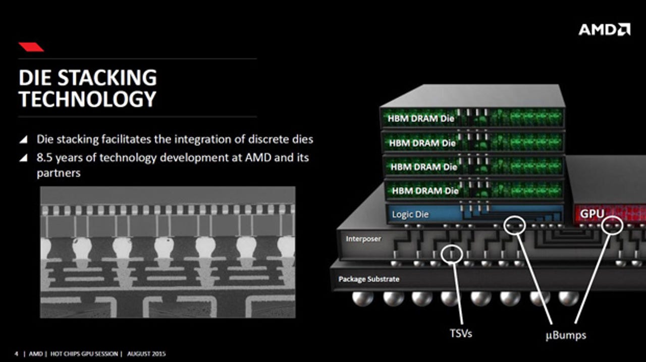
Nearly all AMD and Nvidia graphics cards consist of a GPU surrounded by specialized graphics DRAM (GDDR) memory. The Radeon R9 290X, for example, has up to 16 4Gb chips on the board for a total of 8GB of GDDR5. That takes up lots of space. The Fury and Nano, by contrast, use four 1GB stacks of HBM (four 2Gb chips plus a logic die in each stack) for a total of 4GB. You get less memory, but it has more bandwidth and it uses less power. It also uses significantly less space because the HBM stacks fit next to the chip on the same slice of silicon, known as an interposer. The Fiji GPU itself measures 593 square millimeters and the silicon interposer is 1,000 square millimeters. Even with peripheral circuitry the board area is a fraction of the size of traditional GPUs, and at 7.5 inches the Fury X is 30 percent shorter than the R9 290X.
To make the R9 Nano even smaller, AMD is hand-picking the most efficient chips which can run at lower power, and it moved some of the circuitry onto the back of the card and designed a new cooling system. The result is a 6-inch long board than can fit on a mini-ITX board in a small-form factor PC (though not on Intel's new 5x5 mini motherboard, which doesn't even have a PCI-Express slot). At Hot Chips Macri showed some test results suggesting that while the smaller package will reduce performance a bit, the R9 Nano should still be faster than the R9 290X, and it will be AMD's most efficient card in terms of performance per watt.
Macri also talked a bit about Project Quantum, a 10-inch square PC with dual Radeon R9 Fiji GPUs that is liquid-cooled. He said this should be an ideal platform for virtual reality because it is small and quiet, and the dual GPUs make it possible to use one for each eye. From consumer graphics, HBM will quickly move into other products such as Opteron server processors, he said, and in the long run it could even be used in supercomputers.
The first-generation HBM, which is manufactured by South Korea's SK Hynix, is also just the start, and future version will have higher capacity and greater bandwidth by using denser chips, increasing the number of chips in each stack, and using more total stacks. Both AMD and Nvidia plan to use next-generation HBM in future products. Nvidia has said its Pascal GPU will have up to 32GB of stacked memory at up to 1TB per second.
Next year Samsung also plans to start manufacturing HBM. At the recent Intel Developer Forum, Samsung showed a roadmap for scaling to six 8GB stacks (with eight 8Gb chips each), for a total capacity of 48GB, and increasing the bandwidth to as much as 1.5TB per second. The result should be significantly more powerful PCs and workstations, servers and networking equipment.