Intel shows teraflop chips

Intel chief executive Paul Otellini caused an early stir at the chipmaker's Developer Forum on Tuesday when he briefly showed off a silicon wafer containing chips capable of a trillion floating point operations per second.
The wafer was on show for less than a minute. It contained 80 teraflop chips, which each contained 80 processing cores, alongside some super-fast SRAM. Although it won't be commercially available for another five years, according to Otellini, it represents a massive leap forward on today's technology.
Intel's chief technology officer Justin Rattner gave more details in a later keynote: each 80-core chip measures 22 by 13.75mm, runs at 3.1GHz and has an efficiency of 10 gigaflops per watt. "That's an order of magnitude better than anything today", he said. Each core in the processor is physically stacked on top of 256MB of static RAM, giving a very high level of electronic connectivity and a memory bandiwidth of a terabyte per second.
Ten years ago, the first teraflop computer was built. Called ASCI Red, it contained nearly 10,000 Pentium Pro chips over 1,600 square feet in 85 cabinets and cost around $50m.
Today, Intel is shipping dual-core chips, and hopes to deliver quad-core chips in November. Other manufacturers are further down the multi-core road. The Cell processor, developed by IBM, Sony and Toshiba, contains eight processing cores.
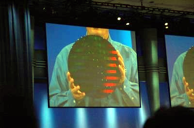
Paul Otellini holds up a magnified image of the
Each core has areas devoted to floating point calculation and communication with the other cores