Researchers develop new method embedding atoms one-by-one to build quantum chip

A team of researchers have developed a new silicon construction technique that could potentially improve the affordability and reliability of building quantum computers.
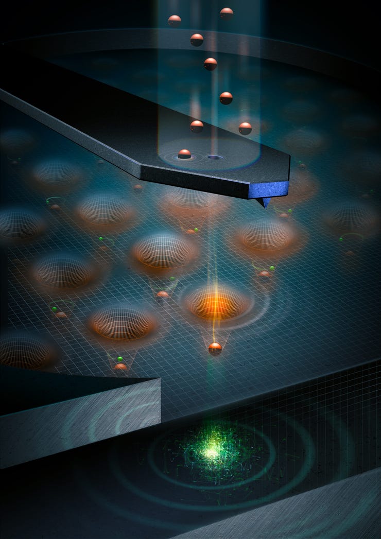
The new technique -- jointly developed by researchers from Australia's University of Melbourne, University of New South Wales (UNSW) and RMIT, and Germany's Helmholtz-Zentrum Dresden-Rossendorf and Leibniz Institute of Surface Engineering -- involves precisely embedding single atoms one-by-one in silicon wafers.
According to the researchers, the technique, which has been published in an Advanced Materials paper, takes advantage of the precision of the atomic microscope, which has a sharp cantilever that "touches" the surface of a chip with a positioning accuracy of just half a nanometre, which is about the same space between atoms in a silicon crystal.
The researchers described how a tiny hole was drilled in the cantilever, so that when it was showered with phosphorous atoms, one would occasionally drop through the hole and embed in the silicon substrate.
A key aspect of this was knowing precisely when an atom was embedded in the substrate so the cantilever could move to the next precise position on the array.
The paper noted that up until now, implanting atoms in silicon has been a haphazard process as when a silicon chip gets showered with phosphorous, an atom would drop in a random pattern, like raindrops on a window. However, the team discovered that it could identify the preciseness through a "click" sound that occurs when an atom drops into the silicon crystal.
"One atom colliding with a piece of silicon makes a very faint click, but we have invented very sensitive electronics used to detect the click, it's much amplified and gives a loud signal, a loud and reliable signal," University of Melbourne professor and lead author David Jamieson said.
"That allows us to be very confident of our method. We can say, 'Oh, there was a click. An atom just arrived. Now we can move the cantilever to the next spot and wait for the next atom.'"
The researchers used equipment including sensitive x-ray detectors, an atomic force microscope that was originally developed for the Rosetta space mission, along with a computer model for the trajectory of ions implanted into silicon, to develop the technique.
Co-author and UNSW Scientia professor Andrea Morello said using this precision and new technique, it would be possible to create a qubit "chip", which can then be used in experiments to test designs for large scale devices.
"This will allow us to engineer the quantum logic operations between large arrays of individual atoms, retaining highly accurate operations across the whole processor," he said.
"Instead of implanting many atoms in random locations and selecting the ones that work best, they will now be placed in an orderly array, similar to the transistors in conventional semiconductors computer chips."
Jamieson added some of the potential large-scale quantum devices that could be developed using the design include unbreakable cryptography and computational drug design, such as rapid development of vaccines.
"We believe we ultimately could make large-scale machines based on single atom quantum bits by using our method and taking advantage of the manufacturing techniques that the semiconductor industry has perfected," he said.
Elsewhere, Archer Materials said it is currently developing a lab-on-a-chip technology that would allow droplets of biological specimens to be analysed and processed using graphene-based sensors. Archer intends to use graphene as an ultra sensitive sensor for detecting and analysing diseases.
In the latest development of this biochip technology, the company said it addressed a key nanotech challenge by successfully integrating a single-atom-thick sheet of graphene with silicon electronics.
According to Archer, the integration was made possible by using an electron beam lithography system to repeatably fabricate the graphene devices.
Archer CEO Dr Mohammad Choucair has described the integration as a "significant" step in the company's biochip development.
"This is the culmination of a lot of strategic planning and coordination involving talented people, world-class facilities, and technology to get to this point," he said. "It's exciting that Archer's 12CQ quantum chip development could also benefit from this latest achievement."
Updated 13 January 2022, 3:03pm (AEDT): Details from Archer Materials added.
More quantum coverage
Australia prioritises 63 critical technologies including quantum and blockchain
AU$70 million will be put into building a new quantum commercialisation hub as part of Australia's Blueprint for Critical Technologies.
Quantum technologies are now part of the military's future roadmap
Defence is exploring how quantum technology can be used as solution for a range of things -- from being an alternative to GPS technology through to securing communications.
Australian industry body calls for more investment in quantum commercialisation
In making recommendations about how to navigate developing innovative tech in Australia, the Australian Information Industry Association has called for additional investment for various tech industries, such as AI and quantum.
Wires above qubits see UNSW researchers take quantum control step
University of New South Wales scientists say latest design could control millions of qubits.