IBM claims breakthrough on carbon nanotubes

Moore's Law has been declared dead many times over the years (most recently in last week's New York Times). But silicon transistors won't last forever, and one of the leading candidates to replace them is a device called a carbon nanotube (CNT).
IBM, which has been working on CNTs for more than a decade, just announced that it has solved one of the major hurdles to using them in practical semiconductors. Although there are many other problems to solve -- both with the basic materials and the device -- it's a step toward commercial production of CNT transistors, perhaps as early as the 5nm node.
AR + VR
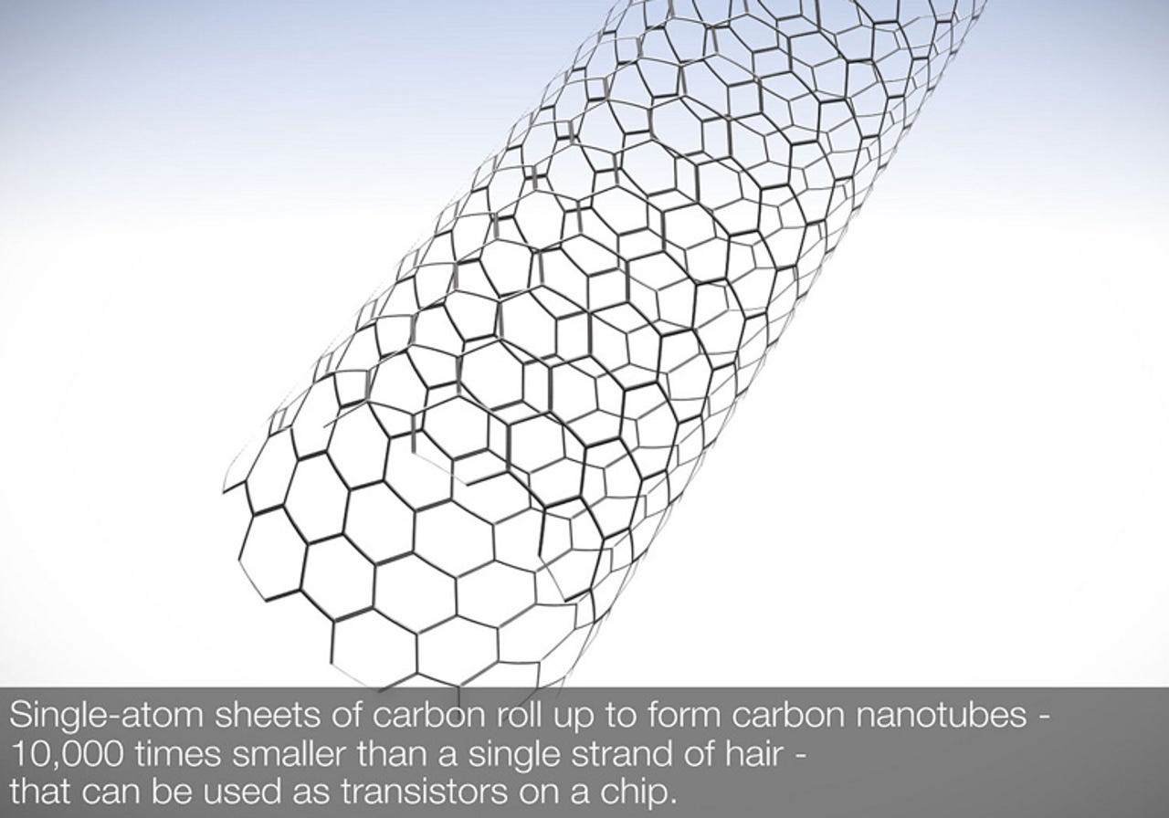
Carbon can form many different allotropes including diamonds, which are an insulator; graphite, a conductor; and graphene, which is a two-dimensional (literally one atom thick) sheet of graphite. The carbon atoms can also bond together to form shapes such as spheres (aka "buckyballs") or tubes known as fullerenes. CNTs, which are essentially rolled-up sheets of graphene, are promising because they are good semiconductors and can easily scale to a few nanometers.
The problem is that the other parts of the transistor need to scale as well including the metal contacts on either side of the channel through which current flows when the transistor is switched on. As the contacts get smaller, the resistance increases, which degrades performance. This is already a big challenge with conventional silicon CMOS transistors at 14nm and above, but it will get worse at future nodes regardless of the transistor type. Dr. Shu-Jen Han, a manager at the IBM T. J. Watson Research Center, said IBM has long understood that the contacts will eventually become the performance bottleneck and began working on a solution for CNTs about three years ago.
To solve this, IBM developed a way to microscopically "weld" tiny molybdenum metal contacts to the end of the tubes, which are arranged horizontally on a substrate. To do this, they pattern two metal electrodes with conventional lithography, "sputter" the metal on the contact regions and then anneal it at a high temperature causing a reaction that welds the metal to the carbon atoms forming a carbide. In IBM's test device, the CNTs have a diameter of 1.2nm and the contacts measure around 9nm. That's already pretty remarkable, but what makes this promising, according to IBM, is that the performance remains the same even as things shrink further. The only real limiter is the lithography to print features at a near molecular level.
There are still plenty of other problems to solve before CNTs will be suitable for volume production. The most fundamental has to do with the material itself. It's still not possible to cost-effectively manufacture highly-pure tubes in volume, and it's a challenge to pack these tiny tubes densely onto a substrate.
But IBM and others are working on this, and Han said that CNTs could be ready to replace silicon in perhaps five to 10 years. "The 5nm node is actually a very interesting node because I've heard many potential solutions, but it is debatable which ones will work," he said. "5nm and 3nm are pretty much non-defined [at this point]."