IBM silicon rejects reborn in solar panels

Just a wafer thin. Yes, indeedy, when the Monty Python crew penned that infamous line in their movie, "Meaning of Life" that hadn't one iota of a clue what it could mean for the solar energy industry.
And now, here's the point of this blog. There's word from IBM this week that they have figured out how to turn scrap semiconductor wafers into material worthy of making silicon-based solar panels.
The reason this is important is because one thing styming faster research and development and deployments in the solar energy industry is a shortage of silicon. IBM figures the new reclamation process will provide a way to reuse the approximately 3.3 percent of all silicon wafers (about 3 million per year) that are started and then discarded during the manufacturing process. Traditionally, these wafers have been ground up and sent to landfills.
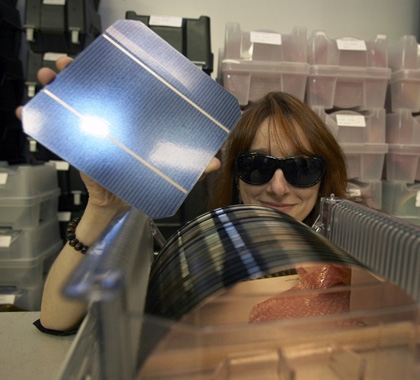
Photo: IBM manufacturing engineer Michelle Bolz holds a solar panel above a crate of scrap wafers ready to be recycled.
The process, developed at the IBM manufacturing facility in Burlington, Vt., has the added bonus of saving on wafer materials procurement need and energy costs, according to IBM. The company intends to share its development with others in the manufacturing industry. Here's a little more background from the National Polution Prevention Roundtable, which recently awarded IBM an innovation prize for its development. Aside from Burlington, IBM is currently bringing the process live in its East Fishkill, N.Y., semiconductor fabrication plant.
