Samsung details roadmap for 2nm chip as it expands foundry capacity

Samsung on Tuesday outlined when it will launch its 2-nanometer (nm) chip process for different applications in the coming years.
The South Korean tech giant said it will begin mass production of 2nm chips for use in mobile applications in 2025, during its Samsung Foundry Forum held in San Jose, California.
Also: These mushroom-based chips could power your devices
This means it will be offering to make application processors used in smartphones and tablets in the 2nm process for customers aiming to launch processors in that size in 2025.
The nm measurement refers to the channel length of the transistors that comprise a chip. Advanced processors have billions of transistors and their channel length being smaller means more transistors can be packed in a single chip, substantially improving their performance.
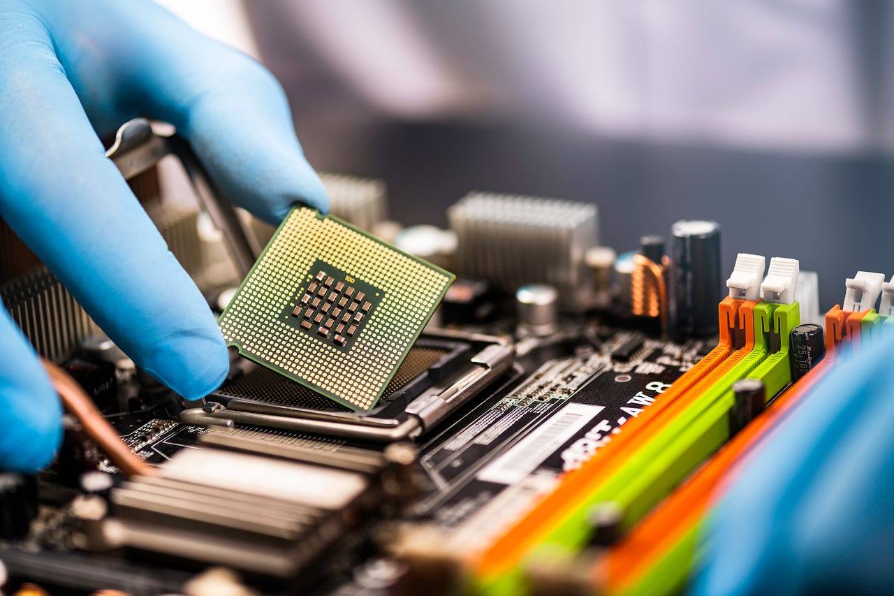
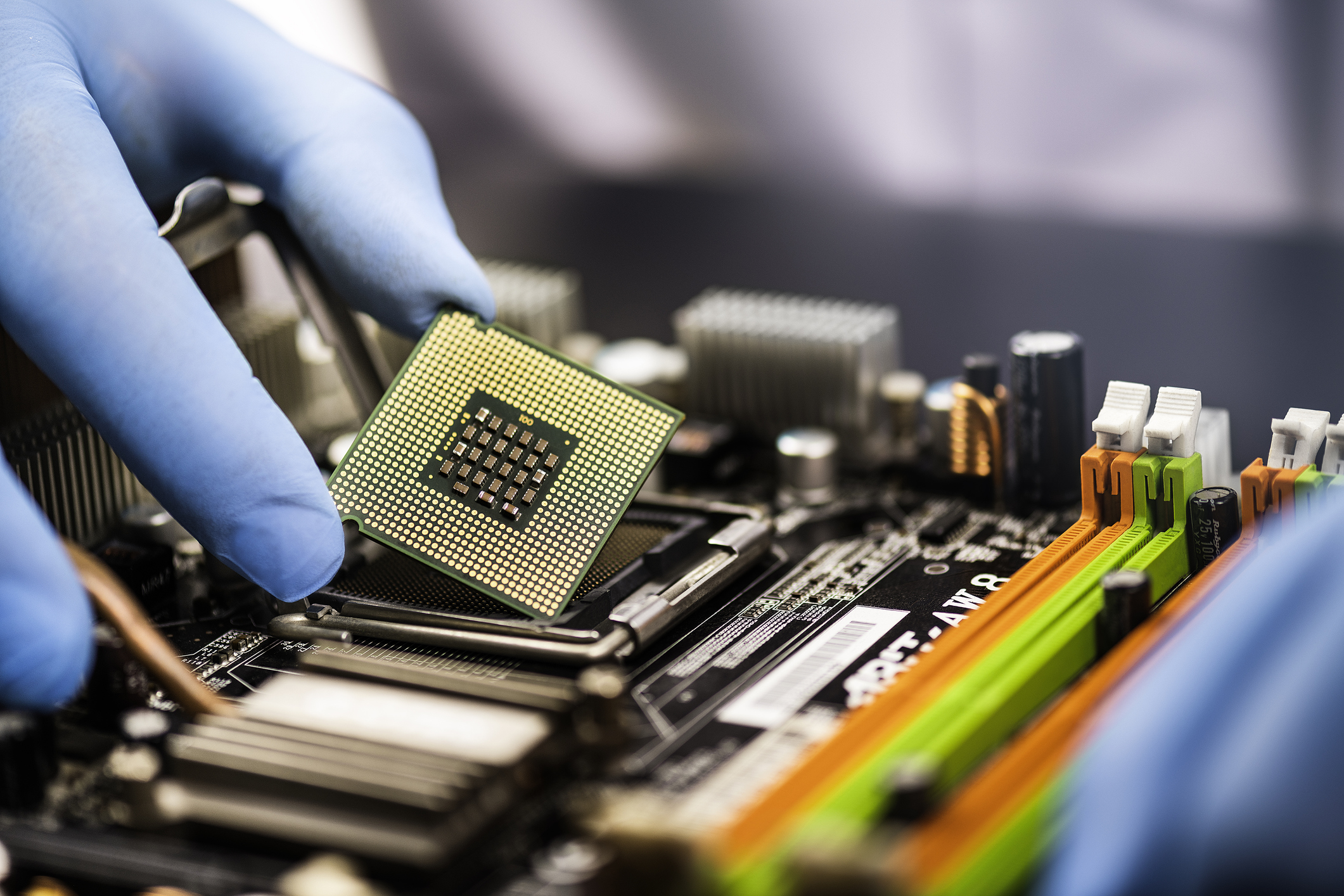
Samsung Foundry, the tech giant's contract chip-producing business unit, offers its manufacturing services to customers such as Qualcomm and Samsung's smartphones business unit.
Also: The best Samsung phones you can buy
After 2025, Samsung said it will offer 2nm chip production for high-performance computing in 2026, and in 2027, offer the process for automotive chips.
The company said its 2nm process has shown a 12% increase and a 25% increase in performance and power efficiency, respectively, compared to its 3nm process, which it launched last year, the first among chipmakers to do so. Samsung said its 2nm process also offered chips that are 5% smaller compared to its 3nm process. The company also said that it will begin mass production of chips using its 1.4nm process in 2027.
In 2025, it will also begin offering contract production for 8-inch gallium nitride (GaN) power management chips as well as 5nm RF chips. It will also begin to offer 8nm and 14nm RF chips for automotive applications.
Also: What is Gallium Nitride (GaN) next-generation charging technology?
Additionally, Samsung is aiming to expand its clean room capacity by 7.3 times by 2027 compared to 2021. This will be achieved through the expansion of its fab in Pyeongtaek -- its most advanced facility to date -- and its new fab being built in Taylor, Texas, the company said. More clean rooms mean it will have more space to execute more orders from customers.
At the forum, Samsung also announced the formation of its Multi-Die Integration Alliance, an alliance with its partners to apply new chip packaging technologies.
Samsung is the world's second-largest contract chip producer after TSMC, which manufactures Apple's A series of chips used in iPhones.