Samsung to spend $15 billion on new advanced chip research complex

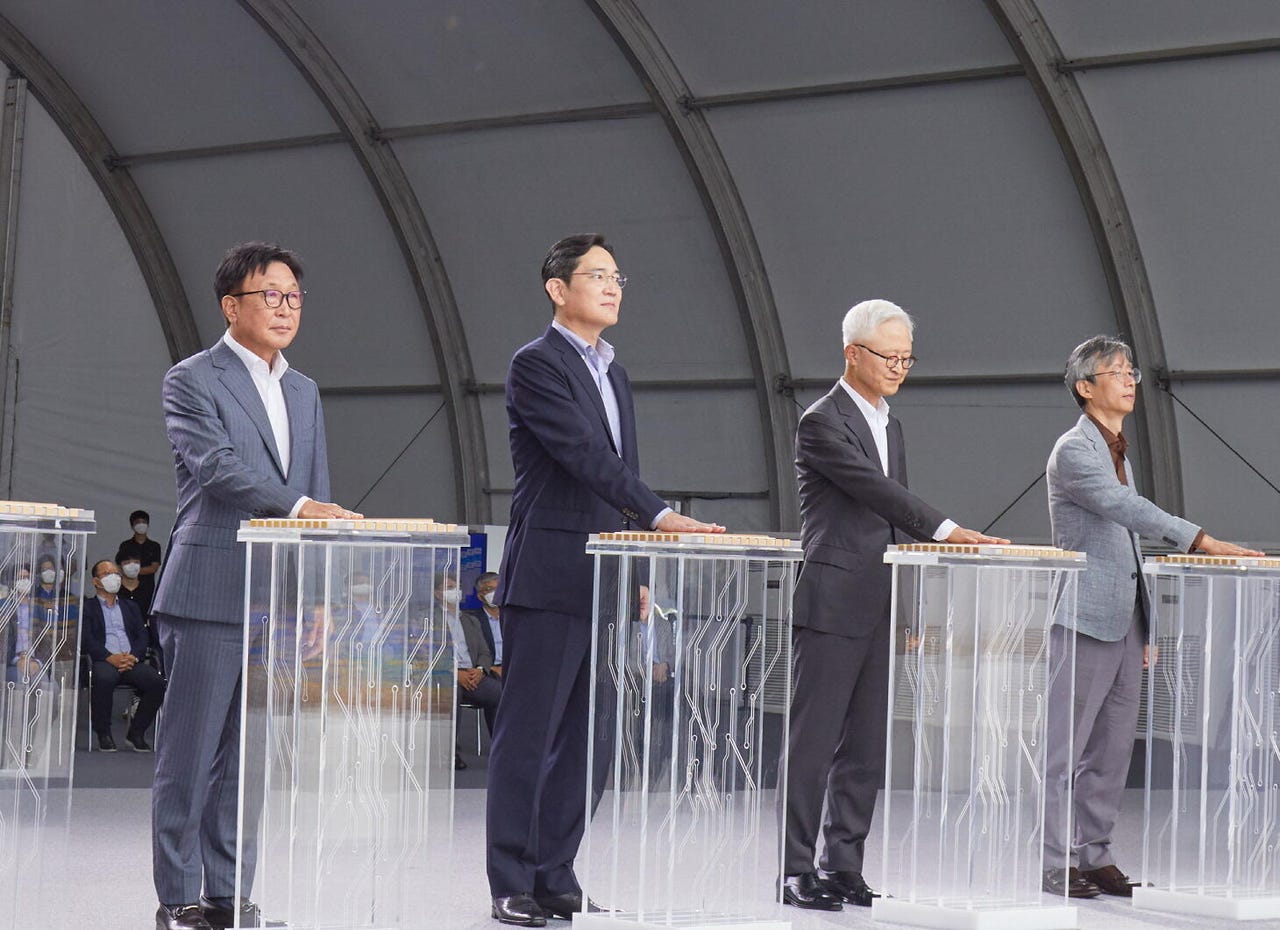
Samsung vice chairman Jay Y Lee, second from left, attended a groundbreaking ceremony for the South Korean tech giant's new advanced chip research complex in South Korea. Image: Samsung
Samsung said on Friday that it will spend 20 trillion won, approximately $15 billion, by 2028 to build a new advanced chip research complex in South Korea.
The new facility to be built at its Giheung campus will lead advanced research on innovative new technologies and new wafer fabrication processes for memory and system semiconductors, the South Korean tech giant said.
The groundbreaking ceremony on Friday was attended by Samsung vice chairman Jay Y Lee, his first official move since he received a presidential pardon last week for his bribery conviction
"We are taking on a new challenge from the very location where we broke ground 40 years ago to build our first semiconductor plant," Lee, the de facto leader of Samsung, told executives and employees at the ceremony.
"If we hadn't made bold R&D investments for next-generation products and in products that came after that, there would be no semiconductor business for Samsung today. We need to continue our tradition of investing preemptively and emphasizing technology," he added.
The facility will cover 109,000 square meters at Samsung's Giheung campus, located just south of Seoul and one of three of the company's major semiconductor production facilities, or fabs, in South Korea. Along with the other campuses in Hwaseong and Pyeongtaek, it manufactures the company's latest chips.
Samsung said it is seeking to "overcome the limits of semiconductor scaling and solidify its competitive edge in semiconductor technology" with the establishment of the complex.
The company noted that its Giheung campus was where in 1992 it developed the world's first 64Mb DRAM, a feat that propelled it to become the world's largest memory chip maker the following year, a position it still holds today.
In June, Samsung announced that it began mass production of chips using its latest 3nm process node. The global chip shortage of the past couple of years has been a boon to Samsung's chip division, as customers stacked up inventory while it also allowed the South Korean tech giant and other contract chip manufacturers to increase their service prices from the surge in demand.
The company's chip division accounted for two-thirds of its operating profit during the second quarter this year. Samsung also noted at the time that in foundry, or contract chip production, it saw its highest revenue for the quarter thanks to improved yield rates.