How Microsoft is making its most sensitive HoloLens depth sensor yet

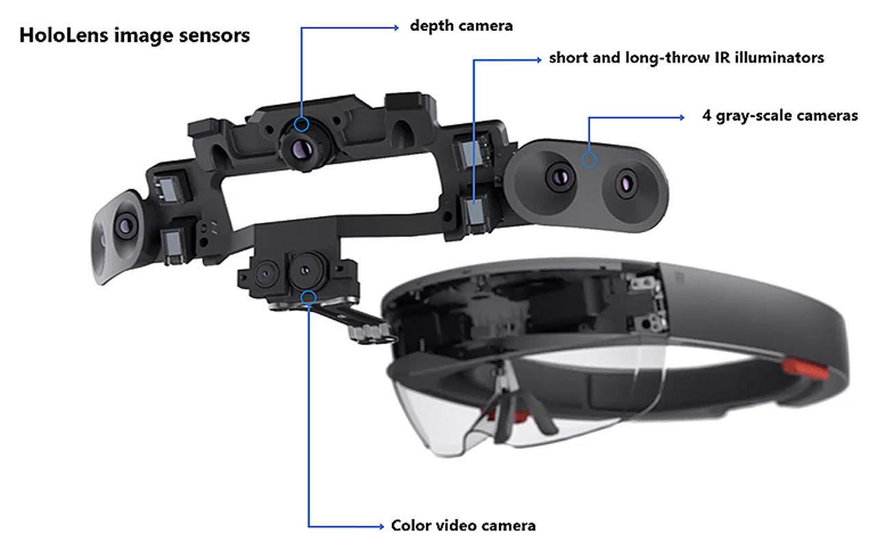
Sensors, including the depth camera, in the original HoloLens.
The next-generation HoloLens sensor is a feat of research and design that crams advanced signal processing and silicon engineering into a tiny, reliable module that Microsoft intends to sell to customers and other manufacturers as Project Kinect for Azure. The company will also use the new sensor in its own products, including the next HoloLens.
More Microsoft
At Build this year, Satya Nadella promised it would be "the most powerful sensor with the least amount of noise", and with an ultra-wide field of view. It's small enough and low-power enough to use in mobile devices. But what does the sensor do, and how will a HoloLens (or anything else using it) 'see' the world into which it mixes 3D holograms?
There are different ways of measuring depth. Some researchers have tried to use ultrasound, while the traditional geometric methods use precisely structured patterns of light, in stereo -- with two beams of light hitting the same object, you can calculate the distance from the angle between the beams. Microsoft has used stereoscopic sensors in the past, but this time took a different approach called 'phased time-of-flight'.
Cyrus Bamji, the hardware architect who led the team to build Microsoft's first time-of-flight (ToF) camera into the Kinect sensor that came with Xbox One, explained to ZDNet how the new sensor works.
It starts by illuminating the scene with a number of lasers, with about a 100 milliwatts of power each, that act like a floodlight. It's uniform everywhere, covers the whole scene at once and turns on and off very quickly.
SEE: Executive's guide to the business value of VR and AR (free ebook)
As the light from the laser bounces off 3D objects like walls and people, it reflects back at the sensor. The distance isn't measured directly by how quickly the light is reflected back (like a radar gun), but by how much the phase of the light envelope that comes back has shifted from the original signal that the lasers emit. Compare the difference in phase (removing any harmonics introduced by minor changes in voltage or temperature to clean up the signal along the way), and you get a very precise measurement of how far away the point is that the light reflected off.
That depth information isn't just useful for scaling holograms to be the right size as you look around in mixed reality; it's also critical for making computer vision more accurate. Think of trick photographs of people pushing over the Leaning Tower of Pizza: with a depth camera you can immediately see that it's a trick shot.
Microsoft's phased time-of-flight sensors are small and thin enough to fit into small mobile devices, and robust enough to go into consumer gadgets that might get knocked around. That's because, unlike stereo vision systems, they're not pricey precision optics that have to be kept in a precise alignment: they can cope with a signal made noisier than usual by the voltage of the electrical current dipping slightly or the equipment warming up, and they use simple calculations that require less processing power than the complex algorithms required for stereo vision calculations.
Depending on how you want to use it, the sensor lets you pick different depth ranges, frame rates and image resolution, as well as picking a medium or large field of view.
The next-generation HoloLens sensor in action at the Microsoft 2018 Faculty Research Summit.
And best of all, phased ToF sensors are silicon that can be mass-produced in high-volume in a fab using standard CMOS processes at low cost. That's just what you need for a consumer product, or something cheap enough to go into large-scale industrial systems.
Small, cheap and fast
The new sensor makes a number of technical breakthroughs: lower power, higher frequency, higher resolution (1,024 by 1,024 pixels), and smaller pixels that determine depth more accurately from further away. Often, improvements in one area mean trade-offs in others -- frequency and distance, for example. "It turns out that if you increase the frequency, you get better resolution; the higher the frequency the less the jitter, but you also get a smaller and smaller operating range," Bamji explains.
A low frequency covers a longer distance from the sensor, but is less accurate. The problem is that while a higher frequency gets more precise results, those results will be the same for multiple distances -- because the readings that come back are with a curve that repeats over and over again. At a frequency of 50MHz, light bouncing off something 3 metres away has the same phase as light bouncing off an object 6 meters or 9 metres away.
The Microsoft team used a clever mathematical trick (called phase unwrapping) to avoid that confusion so they could increase the frequency and also operate at longer distances. The sensor uses multiple different frequencies at the same time and the firmware combines the results. That could be low frequencies that tell you approximately where something is and high frequencies to locate it precisely, or different high frequencies that have different phases so they only line up at one particular distance. That way, says Bamji, "we were able to keep increasing the frequency and get better and better accuracy and still maintain the operating range. We found a way to have our cake and eat it too!"
Phase unwrapping allowed the team to take the frequency of the sensor up from just 20MHz in the earliest research, to 320MHz. Higher frequencies allow the sensor to have smaller pixels, which deliver better depth resolution in the 3D image. The new sensor has high enough resolution to show the wrinkles in someone's clothes as they walk past the camera or the curve of a ping-pong ball in flight -- just 2 centimeters from the centre to the edge -- from a meter away, and all without reducing the performance and accuracy of the sensor the way smaller pixels would do at lower frequencies.
The fourth-generation phased time-of-flight sensor can pick up the curve of a ping-pong ball as it flies through the air.
Small pixels have another big advantage: the sensor itself can be smaller. "If you have small pixels, that brings down the optical stack height," Bamji points out. "Our array is small, which means it can go into devices that are thin."
The new sensor also manages to deliver small, accurate pixels using only one-eighth the power consumption of previous versions (the overall system power is between 225 and 950 milliwatts). It's a trade-off that Bamji characterises as equivalent to Moore's Law. "If you just put in enough power you can get good quality, but for a consumer product that's not good enough. You increase the frequency and that burns more power, but it increases the accuracy and then you decrease the pixel size. As you go through the cycle, you end up where you were but with smaller pixels."
The pixels in the imaging array started out at 50 by 50 microns. That went down to 15 and then 10 microns, and now the pixels are just 3.5 by 3.5 microns each. That's larger than the pixels in a smartphone camera, which are usually 1 to 2 microns square, while the state of the art for RGB sensors is about 0.8 microns square.
On the other hand, the pixels in the Microsoft sensor have a global shutter. Instead of a physical cover that stops any more light coming in, to stop it interfering with the reflected light that's already been captured by the sensor, a global shutter is an extra feature built right into the silicon that tells the sensor to switch off and stop being sensitive to light until it's time to take the next measurement. At the end of 2017, the smallest pixels with global shutters were about 3 microns square, but they didn't have the time-of-flight sensor that this one does.
A complex silicon dance
However, pixels this small can run into quantum mechanical problems with getting electrons to go where you want them to. The sensor detects light by collecting photo charges that it converts into voltages, and those need to be measured precisely.
Bamji compares the problem to inflating a tyre. When you remove the pump and put the cap back on, some air always comes back out. The same thing happens when you reset the part of the sensor where the photo charge is stored: some of the charge can get sucked back in as the reset happens, resulting in what's called kTC noise (that's a shorthand for the formula used to calculate how much noise can get added to the signal). The amount of charge that gets sucked back into the charge varies, so you can't automatically correct for it.
kTC noise only happens where the charge can flow in both directions -- air can come back out of a tyre, but sand can't flow back up into the top half of an hourglass. If there's a complete transfer of the charge, you don't get the noise.
So the Microsoft team gets around the problem by storing the photo charges as what are called minority carriers -- the less common charge-carrying particles in the semiconductor that move more slowly. To convert these charges to a voltage that can be read, they're transferred in what's called a floating diffusion. The sensor resets the floating diffusion and measures the voltage in it immediately after the reset, then moves the photo charge into the floating diffusion and measures the new voltage. Subtracting the first value -- taken right after the reset -- circumvents the problem of kTC noise.
SEE: Sensor'd enterprise: IoT, ML, and big data (ZDNet special report) | Download the report as a PDF (TechRepublic)
The new sensor is the first time-of-flight-system to use this technique, which increases the complexity of silicon engineering required. "But we had to do that because as pixels are becoming smaller and smaller, this problem becomes more and more acute," Bamji explains.
When you get all the way down to each individual (tiny) pixel, it's made up of two interlocking polysilicon 'photofingers' per pixel (earlier generations of the sensor had four or eight fingers, but there's only room for two fingers in the new, smaller pixel).
The fingers take turns to generate a low or high (3.3v) electrical charge. This is a 'drift' field that makes photons drift towards the finger that's generating the high charge faster than they'd normally diffuse across the material. They need to move fast because at the full 320MHz the other finger takes over after 2 nanoseconds and any charges that haven't been captured aren't useful any more. At 320MHz, 78 percent of charges make it all the way to the correct finger.
This finger structure makes the sensors easy to manufacture -- even though few fabs have any experience making this new kind of silicon device -- because it's much less sensitive than other kinds of time-of-flight sensors to any defects in the CMOS process. "We are building a hunk of silicon out of CMOS, but it's unlike the other pieces of silicon on the same chip," Bamji says. "It's a standard CMOS process, but we're building a structure that's unlike any of the other transistors."
In the real world
After all the work to make the pixels smaller, it turns out that smaller pixels aren't ideal for every scene. So to make the sensor more flexible, it can fake having larger pixels by grouping four pixels into one and reading the values from them at the same time (the technical term for that is 'binning'). Which pixel size works best depends on how far away things are and how much of the laser light makes it back to the array in the sensor.
"If you have an object that's close up with plenty of light, you can afford to have small pixels. If you want high resolution for facial recognition, if it's sitting 60cm away from you and you have plenty of light, you want small pixels," says Bamji. "Whereas if you're looking at an object that's very far, at the back of the room, you may not be able to see it accurately with the small pixels and bigger pixels would be better. Where you're starving for laser light, or the laser light has been corrupted by sunlight, you need bigger pixels."
The global shutter helps here, but how much of a problem is sunlight or other ambient light? Sitting in a meeting room on Microsoft's Silicon Valley campus in the afternoon, Bamji estimates the lighting is 200-300 lux; bright sunlight coming in through the window might take it up to 300 or 400 lux. "Our spec is up to 3,000 lux, and the camera functions up to about 25,000 lux. Outdoors on the beach at noon with the sun at full blast somewhere like Cancun, that's 100,000 lux."
Obviously that's something we won't be able to test until products are available, but demos we've seen in normal office environments seem to bear those figures out (and if you were on the beach, you wouldn't be able to see a screen either).
How expensive is this fast, powerful sensor going to be? That depends on manufacturing volumes, but if it's popular enough to be made in large numbers, Bamji expects it to be 'affordable' -- "Affordable, chip-wise, means single digits. This contains silicon and a laser, and in high volumes those are also single digits."
What's still up in the air is what devices beyond HoloLens we'll see the new sensor in, that would sell enough to bring the price down through economies of scale.
Project Kinect for Azure.
Microsoft seems unusually open to selling the sensor to other hardware vendors, but industrial partners are likely to be the first buyers, through Project Kinect for Azure. Imagine an industrial image recognition camera that could see all the way to the back of the fridge for stock checking, with built-in machine learning to recognise what's in the fridge. Devices like that are an ideal example of the 'intelligent edge' that Microsoft is so fond of talking about, and if this sensor could be made at scale as cheaply as say a smartphone camera, we'll see lots of devices that take advantage of precise 3D imaging.
RECENT AND RELATED CONTENT
Microsoft touts HoloLens rentals, business uses for mixed reality
The Microsoft AR/VR pendulum seems to be swinging back toward emphasizing the potential business use of HoloLens and mixed reality headsets.
Microsoft continues its quest for the HoloLens grail
The company remains ahead of a host of competitors with its augmented reality headset, which can justify its expense for mission-critical applications. Mainstream business use, however, will require more than better, cheaper hardware.
Microsoft delivers Windows 10 April 2018 Update for HoloLens
Microsoft is starting to roll out its first Windows 10 feature update for HoloLens since 2016, and is making previews of two new first-party business apps available for the device.
Could the Microsoft HoloLens revolutionize business?(TechRepublic)
Microsoft's HoloLens could transform the enterprise. But what exactly is HoloLens, and why is it unique?
Microsoft HoloLens: Cheat sheet(TechRepublic)
Isn't HoloLens just Microsoft's take on VR headsets? Not at all. Here's what business pros need to know about HoloLens.
Microsoft's next HoloLens may cost less and arrive in early 2019 (CNET)
The next-gen HoloLens is reportedly code-named Sydney.