Gallery: IBM's 3D nanoscale breakthrough makes the world a lot smaller

For more on this story, read Larry Dignan's blog.
Credit: IBM Research - Zurich
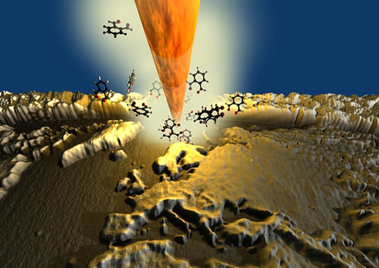
"?The micrograph shows a close-up of the nanoscale silicon tip. This tip, borrowed from atomic force microscopy, measures 500 nanometers in length and only a few nanometers at its apex. It is attached to a cantilever that controllably scans the surface of the substrate material with the accuracy of one nanometer – a millionth of a millimeter. By applying heat and force, the nano-sized tip can remove substrate material based on predefined patterns—operating like a “nanomilling” machine with ultra-high precision."
Credit: IBM Research - Zurich
Credit: IBM Research - Zurich
Credit: IBM Research - Zurich
Credit: IBM Research - Zurich
Credit: Science/AAAS
Credit: Science/AAAS
Credit: Advanced Materials
Credit: Advanced Materials
Compared to existing nanostructuring techniques, such as e-beam lithography, the compact and low footprint IBM tool promises improved and extended capabilities at very small feature sizes, but at five to ten times less cost and far less complexity.
Credit: Michael Lowry, IBM Research - Zurich
Credit: Michael Lowry, IBM Research - Zurich
Credit: Michael Lowry, IBM Research - Zurich
Credit: Michael Lowry, IBM Research - Zurich
Credit: Michael Lowry, IBM Research - Zurich
Credit: Michael Lowry, IBM Research - Zurich