MicroLED displays: Will OLEDs soon be eclipsed?

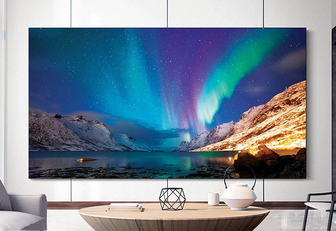
The modular MicroLED-based Samsung Wall.
MicroLED (or mLED, or µLED) is a fast-developing display technology that could take over from OLED (Organic Light Emitting Diode).
Like OLED, MicroLED uses a simple three-colour emissive pixel and delivers very high contrast with deep blacks, a wide colour gamut, high efficiency, fast response, wide viewing angle and the possibility of transparent and flexible (curved) displays. However, MicroLED offers superior gamut, brightness, efficiency and longevity compared to OLED.
Because it uses organic carbon- and hydrogen-based chemistry, OLED is sensitive to degradation by oxygen, moisture and heat. MicroLED, based on inorganic gallium nitride, doesn't have this sensitivity, and so offers long lifetime, lower colour shift with age and no screen burn-in. Also, a modular approach allows the construction of displays of various sizes and shapes, including very large displays.
The basic principle of colour displays -- using large numbers of tiny individual elements, each generating a mixture of just three colours to simulate a full colour image -- hasn't changed in over fifty years. What's changing with increasing rapidity is the technology used to produce the display.
Colour CRT displays were used from 1967 until around 1990 when LCD displays came in. Although Kodak had started developing OLED for camera screens back in 1987, it wasn't until 2004 that the first OLED television was launched. The relative technology spans have been 23 years for colour CRT (although for CRT in general it's roughly 170 years), 30 years and counting for LCD, and 16 years so far for OLED. The once-promising plasma display technology sank without trace in 2014 having lasted for 13 years.
For television and for display screens in general, the problem is always achieving economic, fast and high-yield manufacturing. Until now the manufacturing strategy for LCD and OLED displays has been to lay down each of the layers forming the pixels in a display, whatever the size, in one pass over the entire display area. This may change with MicroLED. Current MicroLED displays use a tiled approach with perhaps as many as 3,600 pixels in an array. These arrays are tested for defects and then stitched together to form a display of the desired size.
MicroLED displays use very small (<100μm) red, green and blue LED chips in a matrix on a backplane.
What are MicroLEDs?
Like OLED, the idea behind MicroLED is as simple as a tristimulus colour display can get: each pixel is made up of three LEDs -- red, green and blue. Very large, relatively low-resolution displays made from discrete LEDs, often used in advertising billboards, have been around for years. However, there are several problems involved in fabricating or assembling very small LEDs (typically less than 100μm) in the very large numbers required -- 8,294,400 pixels x 3 -- for a 4K UHD TV screen. Red, green and blue LEDs all require different and incompatible structures, and each colour runs at different voltages and has different reaction speeds. In addition, the material used to fabricate red LEDs is too mechanically fragile at these small scales.
One approach to structural integration might be to make visible-light blue LEDs with added red and green phosphors -- in much the same way that 'white' LEDs are made by adding a yellow phosphor to a blue LED. Each pixel would comprise one visible blue, one visible blue capped with a red phosphor, and one capped with a green phosphor. The problems of differing structure and drive voltage are solved, because all three LEDs in the pixel are based on a visible blue LED. However, with this approach the blue light is directly emissive, while the red and green light comes from excitation of the phosphors, so the red and green brightness and reaction times differ from the blue.
Micro Nitride, a subsidiary of the Japanese company Nitride Semiconductors, has solved these problems.
Nitride Semiconductors was spun-off from Tokushima University in 2000 to commercially develop research on high-efficiency UV-LEDs, and is now a specialist manufacturer. Micro Nitride has built on the expertise of its parent company to produce Micro UV-LEDs capped with red, green and blue phosphors, all with similar brightness and response times. The base chemistry for the LEDs is gallium nitride (GaN).
SEE: Hiring Kit: Computer Hardware Engineer (TechRepublic Premium)
Another problem for MicroLED is that the smaller the LED, the less light it emits. So the LEDs either have to be made more efficient, or be driven harder (leading to higher power consumption and cooling problems, or both).
Sony was the first company to launch a modular MicroLED display product, called Crystal LED -- previously known as CLEDIS (Crystal LED Integrated Structure) -- in 2016. This achieves very low black levels by placing each MicroLED RGB pixel in the middle of a relatively large black area, and high brightness, presumably by driving a lot of current through each pixel.
These two micrographs of Sony Crystal LED MicroLED pixels -- the second a zoomed in section of the first -- show the large black border around each 0.003mm-square pixel.
A Sony Crystal LED tileable display unit.
The back of a Sony Crystal LED tileable display unit shows substantial cooling and power systems (in comparison, the 'cabinets' of the Samsung Wall are less bulky).
The Sony units measure 403mm by 453mm with a resolution of 320 by 360 pixels. The emitting area is only 1% with a 1.2mm pixel pitch. Prices for a Sony Crystal LED display are currently very high.
There are a number of steps in producing a MicroLED display: fabricating the LEDs, typically on a 4 or 6 inch diameter synthetic sapphire wafer; picking and placing the LEDs onto an active array backplane; testing the individual LEDs in the array,; removing and replacing LEDs that aren't working, and retesting. At present this is a slow, labour-intensive, low-yield process that can take several days. A number of technologies are involved: LED fabrication, backplane fabrication, pick-and-place robotics, and testing and repair using excimer lasers.
Some research has been done into the idea of inkjet-printing OLED displays, but manufacturing currently uses vacuum evaporation through a shadow mask, to form each layer of the entire display area in one pass. Although Samsung has been, for some time, making small AMOLED displays for use in smartphones, LG alone owns the IP and fabrication capacity to manufacture large OLED displays, and has been the sole source for large OLED panels for use in televisions.
The situation with MicroLED is a little different. Inorganic LED technology is well developed, so there's a large knowledge base and a developed manufacturing capability. A fair number of small startup companies have sprung up over the past few years, all attempting to develop their own methods for the various steps in making MicroLED displays. Now these companies are either being bought out by the large display manufacturers, or are providing them with MicroLED modules.
In 2014, Apple bought LuxVue, while Oculus acquired Ireland-based InfiniLED in 2016. Samsung made an unsuccessful bid to acquire PlayNitride in 2017, and Samsung still has close connections with PlayNitride and with Epistar. PlayNitride has expertise in the bulk transfer of MicroLEDs and in fault-testing and repair of MicroLED arrays, while Epistar is the largest Taiwanese manufacturer of LEDs. It seems likely that Epistar is providing Samsung with basic LED technology, and possibly wafers of bulk MicroLEDs, while PlayNitride is building these LEDs into display arrays. PlayNitride calls its array technology PixeLED.
When will MicroLED displays be available?
The frustrating thing for consumers when a new technology shows such huge promise is having to wait until it becomes readily available at a sensible price. Early adopters may find the latest thing is overtaken by yet another new technology -- and being overtaken is exactly what might happen to OLED displays. Although it's difficult to predict the effect the current pandemic may have, given the current state of development it seems likely that MicroLED displays will take a substantial slice of the display market within the next five years.
Market research firm Omdia foresees strong growth in the MicroLED market, led by demand from the smartwatch and TV markets, resulting in shipments of 16.7 million MicroLED displays in 2027:
Meanwhile, IHS Markit predicts that MicroLED shipments will rise from under 1,000 in 2020 to 15.5m by 2026 as manufacturing costs plunge. For example, Samsung supplier PlayNitride has said that it plans to reduce its prices on MicroLED arrays by 95% in the next five years.
TV and smartphone market share
Samsung is the current world leader in television manufacturing and a co-leader (with Huawei) in smartphones, with roughly a 20% market share in both markets. LG, another Korean company, has 12% of the TV market, followed by Japanese company Sony with 7%. LG and Sony both make smartphones, but only have a relatively small market share. In recent years, Chinese companies have been gaining ground, and among them Hisense and TCL are prominent for television manufacture.
Apple has a strong interest in displays, particularly for its smartphone business. The Apple Watch currently uses an OLED screen, supplied by LG. However Apple is planning to switch to a MicroLED display as soon as next year.
Not surprisingly, these are the companies that are investing heavily in new display technologies such as quantum dot, MicroLED and MiniLED.
MicroLED manufacturers
There is already quite a roster of companies involved in developing and making MicroLED elements: Aledia in France, Changelight and HC Semitek in China, Epileds Technologies, PlayNitride, Epistar and Lextar in Taiwan, Glo in Sweden and the US, Iljin Display in Korea, and Micro Nitride and Nichia in Japan.
Inorganic LED technology itself is well established and forms a strong base for these companies to build on. This wasn't the case for OLED.
Samsung Wall modules build up into very large-screen TVs: 16 cabinets in a 4x4 matrix create a 146-inch 4K TV, for example.
The Samsung Wall
Samsung has been showing MicroLED displays at trade shows for several years and distribution partner PSCo showed the Samsung Wall display for the first time in the UK in September 2019 at the Technology Xposed event at Ascot Racecourse.
The Wall is a bespoke MicroLED display currently available to order. Various configurations of Wall display can be built up from almost self-contained rectangular modules, or cabinets, fitted into a frame. Standard cabinet size is 806.4mm by 453.6mm, or 2.64ft by 1.48ft.
Each cabinet contains twelve MicroLED pixel arrays in 4 by 3 configuration. The LEDs in the arrays are Flip-chip, fabricated with the emissive side up, then picked and placed onto a transparent substrate the other way up.
A top edge view and a perspective view of a cabinet from the Samsung Wall display system.
Cabinets are available in three pixel densities, but at the highest density each array is composed of 240 by 180, or 43,200 pixels. The pixels in a cabinet extend up to the cabinet edge, so although on close examination the joint lines between cabinets are visible when the Wall is turned off, image appearance is seamless. Samsung offers the Wall in six frame sizes, from 2.4m by 1.4m up to 12.9m by 7.3m.
The Wall cabinets are currently available in three resolutions: 960 by 540, 640 by 360 and 480 by 270. Pixel pitch is 0.84, 1.26 and 1.68 millimetres, which may seem quite large but must be considered in relation to the size of the final image once the modules are assembled into a display.
For example, a 3.2-by-1.8m Wall (146 inches on the diagonal) configured as a 16:9 aspect ratio 4K television would be composed of 16 cabinets in a 4 by 4 matrix. Using the 960-by-540 cabinets provides a resolution of 3,840 by 2,160 which is actually 3.84K horizontal, known as Ultra HD or UHD. The cabinets are rated at 100,000 hours lifetime.
The previously mentioned Sony Crystal LED system is a similar modular product.
Incumbent display technologies fight back?
Manufacturers of UHD LCD televisions could retaliate by improving their technology while offering lower prices than MicroLED. UHD HDR LCD could be what it always should have been by massively increasing the number of backlight dimming zones. Current TVs are often confusingly referred to as 'LED TVs' simply because they use LED backlighting. Most UHD HDR LCD televisions only notionally offer High Dynamic Range by locally dimming the backlight over a small number of large areas, rather than anything approaching a pixel-by-pixel basis. This results in ineffective contrast management and an annoying halo effect around bright images on a black background. At CES 2020, Chinese manufacturer TCL, relatively unknown in the UK, unveiled its Vidrian technology based on MiniLED -- 25,000 individual backlight LEDs divided into 1,000 dimming zones. Samsung is apparently planning to launch a range of MiniLED backlight TVs in 2021.
Today in the UK you can buy a 65-inch TCL 8 series 4K (2160p) UHD, HDR LCD Smart (Roku OS) TV with a MiniLED backlight and Quantum Dot colour for around £1,500.
Meanwhile, OLED is hamstrung by the problems inherent in its organic chemistry. Initial hopes for OLED were that tweaks to the chemistry would extend its lifetime. Recent firmware changes to OLED image management systems have reduced image burn-in, but the basic problem is still there. Even LG, which had pinned its future in the television market on OLED, has started investing in MicroLED, exhibiting a 145-inch MicroLED display at the CES 2020 show in January.
MicroLED is likely to face scaling problems as far as smaller high-resolution displays -- such as those used for computer monitors -- are concerned. There is a limit on just how closely together individual MicroLEDs can be packed together by pick and place methods. Unlike LCD and OLED, the manufacturing cost of MicroLED displays is directly related to the number of LEDs used, so cost does not fall as screen size is reduced, for the same resolution.
Current plans for MicroLED focus on the large-screen TV market and on smartphone displays at lower resolutions. It seems likely that the older LCD technology will coexist with MicroLED for some years to come, particularly for low-cost medium to small screen sizes. The future for OLED seems less certain.
RELATED CONTENT
CES 2020: Samsung expands MicroLED TV home lineup
Samsung unveils 219-inch MicroLED display
Samsung researching quantum dot on MicroLED TVs
CES 2020: LG targets selling 6 million OLED TV panels
Apple developing own MicroLED screens for Apple Watch using secret facility